Troubleshooting Ground Bounce Pitfalls in 6-Layer Custom PCBA for Diagnostic Equipment
Troubleshooting Ground Bounce Pitfalls in 6‑Layer Custom PCBA for Diagnostic Equipment When High-Frequency Diagnostic Signals Expose Ground Bounce in 6‑Layer PCBAs Diagnostic instruments—ultrasound fr...
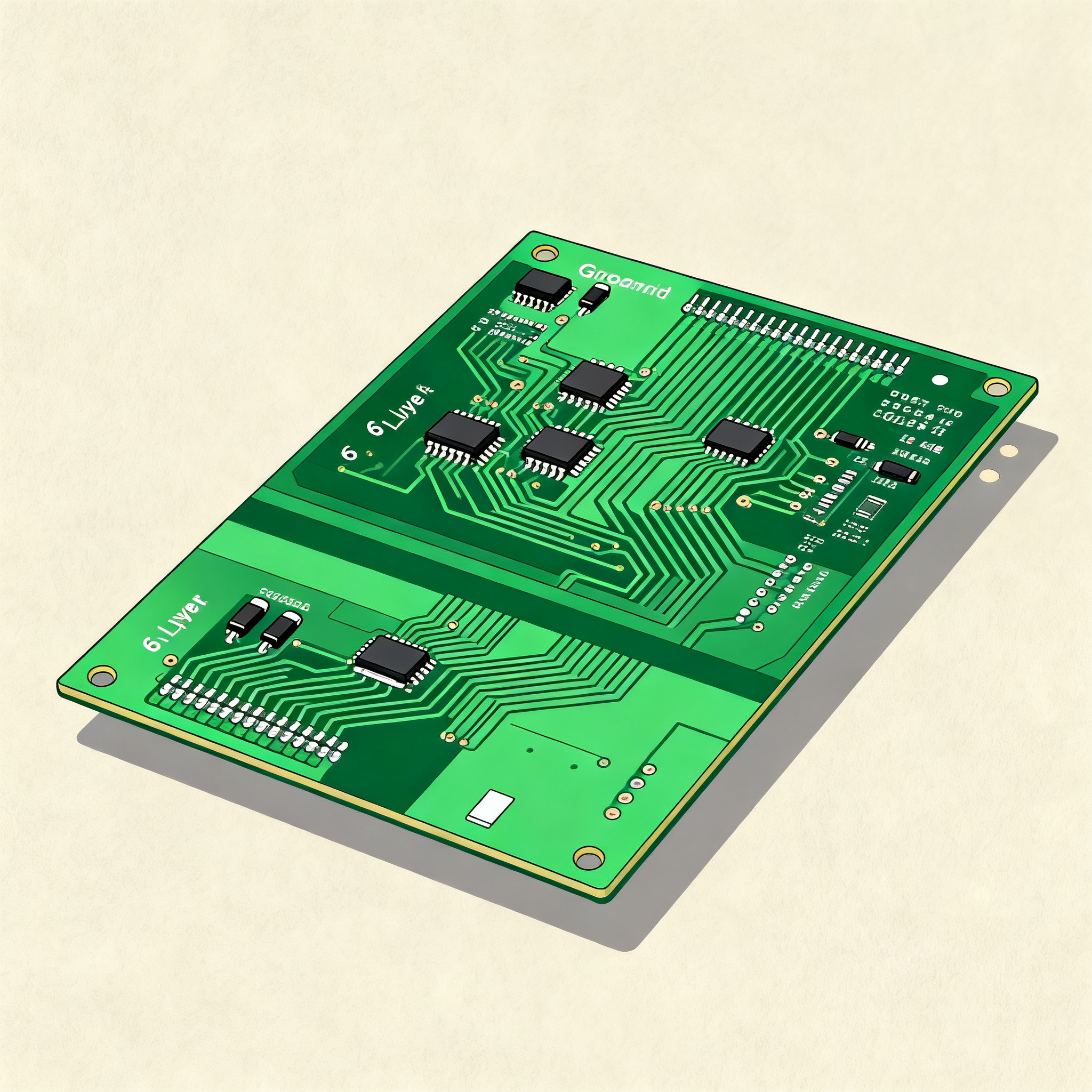
Troubleshooting Ground Bounce Pitfalls in 6‑Layer Custom PCBA for Diagnostic Equipment
When High-Frequency Diagnostic Signals Expose Ground Bounce in 6‑Layer PCBAs
Diagnostic instruments—ultrasound front‑ends, 12‑lead ECG monitors, pulse oximetry modules, and high‑speed data acquisition cards—routinely push clock and data rates past 50 MHz. At these frequencies, the benign ground reference you measure with a DC multimeter turns into a dynamic, bouncing node that corrupts analog measurements and flips digital thresholds. Low‑frequency designs rarely exhibit signal integrity problems, but as edge rates sharpen and bus speeds climb, ground bounce, crosstalk, and ringing dominate the failure landscape.
In a 6‑layer custom PCBA, the problem intensifies because you have multiple signal layers sharing a limited number of reference planes. A split power plane, a gap in the ground pour, or a poorly placed via can force return currents to detour, creating large loop inductances that translate every switching event into a voltage spike on the ground net. Common PCB failure modes—intermittent resets, false triggers, and drifting ADC readings—often trace back to ground bounce that goes undetected during bench validation. For an OEM building diagnostic equipment, a board that passes functional test but fails in the field because of occasional ground‑bounce‑induced bit errors is a costly recall waiting to happen.
This article walks you through the physics, compares the two dominant mitigation philosophies, and gives you a field‑tested troubleshooting workflow that catches ground bounce before it reaches the patient. Every recommendation is tailored to the 6‑layer stackups that dominate portable and cart‑based diagnostic systems, where cost, layer count, and signal density must be balanced against measurement integrity.
How Simultaneous Switching Noise Corrupts Measurement Accuracy in 6‑Layer Stackups
Ground bounce is simultaneous switching noise (SSN) appearing on the ground reference. When dozens of CMOS outputs inside an FPGA or microcontroller switch state, the transient current di/dt flows through the parasitic inductance of bond wires, package leads, and PCB traces. The voltage developed across that inductance—Vbounce = Leff × di/dt—momentarily lifts the local ground potential. All ground points on a circuit board assembly should be at the same potential, but inductance makes that impossible during switching transients.
In a 6‑layer diagnostic board, the stackup geometry dictates how much of that bounce reaches sensitive analog front‑ends. Continuous ground planes and bypass capacitors placed close to ICs are the first line of defense, but even a solid plane can exhibit cavity resonances and edge reflections if the return path is not managed layer‑by‑layer. The external effects are just as critical: ground bounce forces the circuit ground potential below 0 V, forward‑biasing ESD protection diodes and causing latch‑up in sensitive CMOS structures.
The table below compares four common 6‑layer stackups and their inherent susceptibility to ground bounce in diagnostic applications. The numbers assume a 100 MHz digital bus with 8 simultaneously switching drivers and a 1 ns rise time.
| Stackup Type | Layer Sequence (1–6) | Ground Plane Arrangement | Return Path Discontinuity Risk | Typical Ground Bounce (mVpp) | Suitability for Diagnostic Equipment |
|---|---|---|---|---|---|
| Signal‑Ground‑Signal‑Signal‑Power‑Signal | S1‑G2‑S3‑S4‑P5‑S6 | Single ground on L2; signals on L3, L4 reference L2 and P5 | High when L4 signals cross split power shapes | 40–80 | Poor for mixed‑signal; avoid unless all high‑speed traces stay on L1/L3 |
| Signal‑Ground‑Signal‑Power‑Ground‑Signal | S1‑G2‑S3‑P4‑G5‑S6 | Two grounds (L2, L5); tight coupling to adjacent signal layers | Low if stitching vias are placed near signal transitions | 15–35 | Excellent for mixed‑signal diagnostic boards; isolate analog on L1/L3 |
| Signal‑Signal‑Ground‑Power‑Signal‑Signal | S1‑S2‑G3‑P4‑S5‑S6 | Single ground on L3; high‑speed signals on L1/L2 have no adjacent reference | Very high; return currents must travel through vias to L3 | 80–150 | Not recommended for any design above 25 MHz |
| Signal‑Ground‑Power‑Signal‑Ground‑Signal | S1‑G2‑P3‑S4‑G5‑S6 | Two grounds sandwiching power; signals on L1, L4, L6 | Moderate; L4 signals reference P3, need decoupling to maintain low impedance | 20–50 | Good when high‑speed digital is confined to L1/L6 and analog to L4 |
The stackup with two ground planes (G2 and G5) consistently delivers the lowest ground bounce because it provides a low‑inductance return path for every signal layer. However, simply adding a second ground plane is not a panacea. If the planes are not stitched together with a dense via fence along the board periphery and near high‑speed connectors, cavity resonances can amplify bounce at certain frequencies. In one ECG monitor design we analyzed, a 120 MHz clock harmonic excited a parallel‑plate resonance between the two ground planes, producing 60 mV of ground bounce on the ADC ground pin despite a textbook stackup. The fix was a ring of ground vias spaced λ/10 apart, which suppressed the resonance without changing the layer count.
Stackup Integrity vs. Decoupling Placement: Which Mitigation Strategy Protects Diagnostic PCBs Best?
Engineers often split into two camps when tackling ground bounce: those who swear by an uninterrupted, low‑inductance ground plane as the universal remedy, and those who invest heavily in a meticulously designed decoupling network. In reality, diagnostic equipment demands a blend of both, but the starting point matters. Sierra Circuits emphasizes that avoiding slots and gaps in the ground plane is the most effective single step you can take. PCBBUY’s five‑method approach, on the other hand, focuses on capacitor selection, placement, and power‑delivery network (PDN) impedance profiling. AllPCB’s analysis of noise margin erosion shows that ground bounce directly eats into the threshold windows of both input and output stages, making the choice of mitigation strategy a direct determinant of measurement accuracy.
The comparison table below helps you decide where to invest your design effort when working with a 6‑layer diagnostic board that must capture microvolt‑level biopotentials while processing megapixel image data.
| Comparison Metric | Stackup Integrity Approach (Sierra Circuits) | Decoupling Placement Approach (PCBBUY) | Selection Criteria & Failure Boundary |
|---|---|---|---|
| Primary Focus | Uninterrupted ground planes; minimize loop inductance through geometry | Local charge delivery; minimize PDN impedance across frequency | Choose stackup integrity when return path discontinuities dominate; choose decoupling when IC di/dt is the main aggressor |
| Key Technique | Route all high‑speed traces over solid ground; avoid splits under clocks and data buses | Place multiple capacitor values (100 nF, 10 nF, 1 nF) within 2 mm of power pins; use buried capacitance layers | If a trace crosses a split, no capacitor can fix the resulting loop; if the PDN impedance peaks at a clock harmonic, even a perfect plane won’t suppress the bounce |
| Impact on Diagnostic Accuracy | Reduces common‑mode ground shift, preserving ADC linearity and CMRR of instrumentation amplifiers | Minimizes supply ripple that couples into analog stages, preventing false switching and baseline wander | For a 16‑bit ADC, ground bounce must stay below 38 µVpp to remain within 1 LSB; both strategies are needed to achieve this |
| Implementation Complexity | Requires careful floorplanning and possible layer re‑assignment; fewer BOM changes | Demands dense BOM and precise placement; easier to retrofit on an existing layout | Start with stackup optimization; add decoupling as a tuning step during PDN simulation |
| When to Prioritize | Boards with multiple high‑speed buses crossing domain boundaries; mixed‑signal designs where analog and digital share a ground | Boards with dense BGAs, high pin‑count FPGAs, or limited routing space that forces signal layers away from reference planes | If ground bounce exceeds 50 mV on the ADC ground, re‑evaluate the stackup before adding more capacitors |
Tip: In diagnostic equipment, the most cost‑effective sequence is to lock in a low‑inductance stackup first—preferably the S‑G‑S‑P‑G‑S configuration—and then use a PDN analyzer to place decoupling capacitors exactly where the impedance profile shows peaks. This dual approach addresses both the geometry‑driven and the transient‑current‑driven components of ground bounce. Remember that ground bounce forces the external ground potential below 0 V, so even a perfectly decoupled IC can still suffer if the board‑level return path is inductive.
Step‑by‑Step Troubleshooting: Pinpointing and Fixing Ground Bounce in 6‑Layer Diagnostic Assemblies
When a diagnostic board exhibits intermittent false readings, the root cause is rarely obvious. A structured troubleshooting approach, combining visual inspection, targeted probing, and systematic isolation, turns a PCBA nightmare into a solved case. The workflow below draws on field‑proven techniques from EBest PCB’s troubleshooting guide and Sierra Circuits’ layout rules, adapted specifically for 6‑layer diagnostic assemblies.
| Symptom | Likely Root Cause | Diagnostic Method | Corrective Action |
|---|---|---|---|
| ADC readings fluctuate in sync with digital bus activity | Ground bounce on the analog ground pin | Probe the ADC ground pin with a 1 GHz differential probe while toggling a digital I/O bank; look for spikes >10 mV | Add a ferrite bead or 0 Ω resistor to create a single‑point analog ground island; ensure no digital traces cross the analog ground region |
| Intermittent false triggers in comparator or Schmitt‑trigger inputs | Ground bounce exceeding the noise margin of the logic family | Capture the ground waveform at the comparator’s ground reference; compare with the input signal | Reroute high‑speed traces away from the comparator; add a local 100 nF capacitor directly between VCC and ground at the comparator package |
| Elevated EMI at specific harmonics during radiated emissions testing | Return current loops radiating from discontinuous ground planes | Use near‑field H‑field probes to map hot spots; correlate with clock frequencies | Stitch ground planes with vias every 5 mm along board edges; ensure no clock trace crosses a plane split; add series termination to slow edge rates |
| System resets or latch‑up when motors or relays switch | Inductive kickback coupling into the digital ground net | Trigger an oscilloscope on the relay driver signal and monitor the microcontroller ground pin | Add TVS diodes across inductive loads; route high‑current return paths on a separate power ground plane that joins the digital ground at a single star point |
| Unexplained baseline wander in ECG or EEG front‑ends | Low‑frequency ground bounce caused by PDN resonance | Perform an impedance sweep of the power rail using a vector network analyzer; look for peaks below 100 kHz | Increase bulk capacitance (10–100 µF) near the analog supply; use a low‑ESR tantalum or polymer capacitor to damp the resonance |
Once you’ve identified the offending net, follow this sequence to eliminate ground bounce without a full board respin:
- Map the return path. Overlay the signal layer onto the adjacent reference plane in your CAD tool. Any area where the reference plane is voided, split, or more than one dielectric thickness away is a suspect discontinuity.
- Probe the ground locally. Use a high‑bandwidth differential probe with the negative lead connected to a quiet ground point (e.g., the power supply return) and the positive lead touching the IC ground pin. A spike of more than 5% of the supply voltage during switching events confirms ground bounce.
- Add local decoupling. Place a 100 nF X7R capacitor in 0402 package directly across the power and ground pins of the offending IC, using the shortest possible traces. For BGAs, use via‑in‑pad to connect to the buried capacitance layer.
- Reroute critical traces. If a high‑speed clock or data line crosses a plane split, move it to a layer that has a continuous reference plane. If that’s impossible, bridge the split with a stitching capacitor (10–100 nF) to provide an AC return path.
- Verify with simulation. Before ordering new boards, run a quick SI/PI simulation using extracted parasitics. Even a simple SPICE model with estimated Leff and di/dt can confirm whether your fix brings Vbounce below the ADC’s noise budget.
When you’re ready to prototype the revised 6‑layer diagnostic board, NovaPCBA’s assembly service ensures that decoupling capacitors are placed with sub‑millimeter precision and that controlled‑impedance traces meet your stackup specifications. A clean layout is only as good as the assembly that executes it.
Ground Bounce in Diagnostic PCBAs: Senior Engineers’ Questions Before Tape‑Out
Q: Can ground bounce cause intermittent false readings in a 12‑lead ECG front‑end, and how do I isolate it?
A: Yes. Ground bounce shifts the reference voltage of the instrumentation amplifier and ADC, producing baseline wander or missed R‑waves that mimic electrode contact issues. To isolate it, inject a known 1 mV, 10 Hz test signal into the front‑end while the digital back‑end runs a memory test that toggles all data buses. Probe the ADC’s ground pin with a high‑bandwidth differential probe (≥500 MHz) referenced to the system’s star ground. If you see spikes synchronous with the bus activity, ground bounce is the culprit. Temporarily halting the digital activity should make the noise disappear, confirming the diagnosis.
Q: What is an acceptable ground bounce voltage for a 16‑bit ADC in a diagnostic instrument?
A: For a 16‑bit ADC with a 2.5 V reference, 1 LSB equals 2.5 V / 65,536 ≈ 38 µV. To keep ground‑bounce‑induced errors below 1 LSB, the peak‑to‑peak bounce on the ADC’s ground pin must stay under 38 µV. In practice, achieving that at the die is nearly impossible on a 6‑layer board with fast digital logic. Instead, aim for less than 10 mVpp on the PCB ground plane and rely on differential inputs, local decoupling, and a clean analog ground island to prevent the bounce from appearing as a differential signal at the ADC input. The ADC’s power‑supply rejection ratio (PSRR) will further attenuate the remaining common‑mode noise.
Q: Should I use a 6‑layer board with two ground planes to reduce bounce, or is one solid plane enough?
A: A single solid ground plane on layer 2, paired with a continuous power plane on layer 5, often suffices for diagnostic boards operating below 200 MHz. This configuration gives every signal layer an adjacent reference, provided you route high‑speed traces only on layers 1, 3, and 6. Add a second ground plane (e.g., S‑G‑S‑P‑G‑S) only if you have high‑speed buses crossing split power domains or if EMI pre‑compliance scans show excessive radiation from the board edges. The second plane adds cost and weight but can reduce ground bounce by an additional 10–15 dB when stitched correctly.
Q: How can I simulate ground bounce in pre‑layout analysis without expensive 3D field solvers?
A: Use SPICE models of your IC output buffers combined with extracted PCB parasitics (R, L, C) of the power delivery network. Tools like Cadence Sigrity or Siemens HyperLynx can run fast SI/PI simulations on a pre‑layout netlist. For a quick first‑order check, estimate the simultaneous switching noise using Vbounce = Leff × di/dt. Leff is the total inductance from the IC ground pin to the board’s star ground—typically 1–5 nH for a well‑designed 6‑layer board. di/dt can be approximated from the driver’s output current and rise time. If the calculated bounce exceeds your ADC’s noise budget, you know you need to lower inductance or slow edge rates before layout begins.
Q: What is the most common layout mistake that triggers ground bounce in 6‑layer diagnostic boards?
A: Routing high‑speed digital traces over a split in the ground plane. When a trace crosses from one ground region to another, the return current must detour around the gap, creating a large loop that radiates and induces a voltage spike on the ground net. In a 6‑layer board, this often happens when a designer places a connector or an isolation barrier that cuts the ground plane, then routes SPI or parallel bus lines across the cut. Always maintain a continuous reference plane under critical signals. If a split is unavoidable, bridge it with a stitching capacitor to provide a low‑impedance return path at the frequencies of interest.
Q: When does it make sense to move from a 6‑layer to an 8‑layer stackup solely for ground bounce mitigation?
A: Move to 8 layers if you’ve exhausted decoupling and routing optimizations and still measure more than 50 mV of ground bounce on the ADC ground pin, or if you need to isolate noisy digital and sensitive analog domains without compromising plane continuity. An 8‑layer board lets you dedicate two full ground planes—one for digital, one for analog—and still have room for multiple signal and power layers. The additional cost (typically 20–30% over a 6‑layer board of the same size) is justified when the diagnostic instrument’s regulatory approval or clinical accuracy depends on achieving sub‑10 mV ground bounce across all operating modes.
Ground bounce is not a theoretical concern; it’s a measurable, repeatable failure mechanism that directly impacts patient diagnostic data. By selecting the right 6‑layer stackup, verifying return path continuity, and using a methodical probing workflow, you can catch and eliminate bounce before it escapes into production. When you need a manufacturing partner who understands the nuances of high‑precision diagnostic PCB assembly, NovaPCBA offers controlled‑impedance processing, micro‑via capability, and rigorous incoming inspection to ensure your carefully engineered stackup performs in the real world.
References & Further Reading
- Reducing Ground Bounce in PCB Assembly – Sierra Circuits
- PCB Issue Guide: PCB Failure Analysis and Common Issues – MCL
- 6 Common Causes of PCB Failure: What OEMs Should Know – Matric
- Troubleshooting PCBA Nightmares: A Practical Guide for Engineers – AllPCB
- How to Reduce Ground Bounce in PCBA Process through 5 Effective Methods – PCBBUY
- How to Eliminate Ground Bounce in PCBA Process of Guidelines – PCBBUY
- Ground Bounce in PCB Design: Causes, Effects, and Mitigation Strategies – AllPCB
- PCB Troubleshooting Guide – EBest PCB
- How to reduce ground bounce in PCB – Andwin Circuits
- NovaPCBA – Custom PCB Assembly Services