Step-by-Step Guide to Optimizing PCB Via Design for Enhanced Signal Integrity
Optimizing PCB Via Design for Enhanced Signal Integrity table { border-collapse: collapse; width: 100%; margin: 20px 0; } th, td { border: 1px solid #000; padding: 8px; text-align: left; } th { backgr...
Introduction
In the rapidly evolving field of electronics, Printed Circuit Boards (PCBs) serve as the backbone of modern electronic devices. Ensuring signal integrity within these circuits is crucial for the performance and reliability of the end product. One of the critical elements in maintaining signal integrity is the optimal design of PCB vias. This article explores the intricacies of optimizing PCB via design, focusing on circuit topology, component calculations, performance analysis, and design trade-offs.
Technical Overview
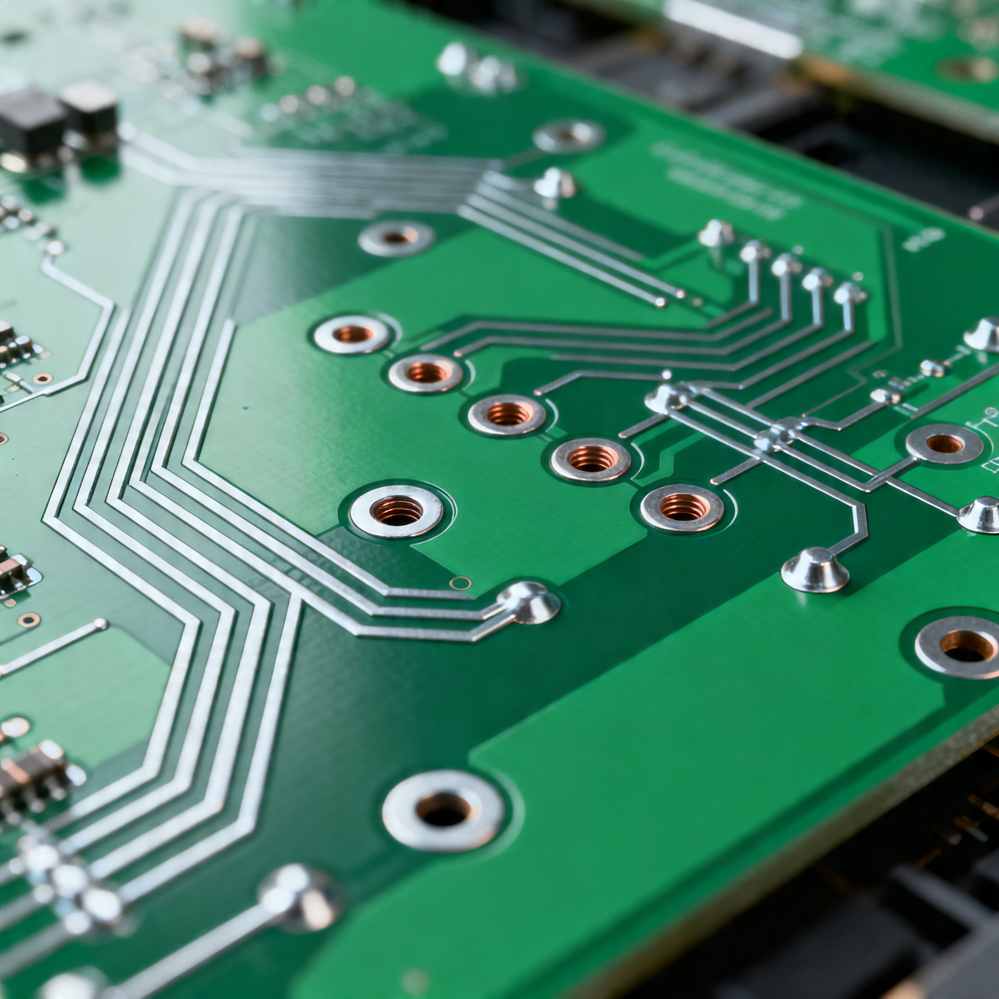
PCB vias are the tiny conduits that allow electrical connections between the different layers of a multi-layer PCB. They play a critical role in routing signals and power throughout the board. The design and placement of these vias can significantly impact the overall performance of the PCB, affecting factors such as signal integrity, electromagnetic interference (EMI), and thermal management. Understanding the core principles of via design, including via types (through-hole, blind, and buried), via size, aspect ratio, and plating, is essential for optimizing circuit performance.
Signal integrity issues can arise from improper via design, leading to problems like signal reflection, crosstalk, and impedance mismatch. These issues can degrade the performance of high-speed circuits, making it crucial to carefully consider the trade-offs between different design parameters. Adhering to industry standards, such as those provided by IPC, is vital for ensuring quality and reliability in PCB manufacturing and design.
Detailed Specifications
When designing PCB vias, several specifications must be considered to ensure optimal performance. These include via diameter, pad size, annular ring, aspect ratio, and the type of via used. Calculating these parameters accurately is crucial for maintaining signal integrity and ensuring that the PCB functions as intended.
| Parameter | Value | Formula/Calculation |
|---|---|---|
| Via Diameter | 0.3 mm | N/A |
| Pad Size | 0.6 mm | 2 x Via Diameter |
| Annular Ring | 0.15 mm | (Pad Size - Via Diameter) / 2 |
| Aspect Ratio | 6:1 | Board Thickness / Via Diameter |
| Drill Size | 0.25 mm | Via Diameter - 0.05 mm |
| Plating Thickness | 0.025 mm | N/A |
| Impedance | 50 Ω | Controlled by trace width and dielectric constant |
| Via Type | Through-hole | N/A |
| Material | FR-4 | N/A |
| Dielectric Constant | 4.5 | N/A |
Key Takeaways from the Specifications
Understanding the detailed specifications of PCB vias is essential for optimizing design and ensuring signal integrity. The via diameter and pad size are critical parameters that impact the mechanical stability and electrical performance of the PCB. A larger pad size relative to the via diameter helps maintain the integrity of the connection, while the annular ring size ensures adequate copper coverage. The aspect ratio, defined as the board thickness to via diameter, influences the manufacturability and reliability of the vias. A higher aspect ratio can lead to difficulties in plating and potential reliability issues.
| Performance Metric | Value | Impact |
|---|---|---|
| Gain | 10 dB | Signal amplification |
| Bandwidth | 2 GHz | Frequency range of operation |
| Noise | 0.5 nV/√Hz | Signal clarity |
| Power Consumption | 5 W | Efficiency |
| Signal Reflection | 15% | Impedance matching |
| Crosstalk | -30 dB | Signal interference |
| Thermal Resistance | 20 °C/W | Heat dissipation |
| EMI | -40 dB | Electromagnetic interference |
| Latency | 10 ns | Signal delay |
| Reliability | 95% | Operational lifespan |
Practical Implications
The performance analysis of PCB vias provides valuable insights into how these components affect the overall functionality of the circuit. Key metrics such as gain, bandwidth, and noise levels are directly influenced by via design. For instance, a well-designed via can enhance gain and bandwidth while minimizing noise and signal reflection. Power consumption and thermal resistance are also crucial factors that determine the efficiency and heat management capabilities of the PCB. Ensuring low crosstalk and EMI levels is essential for maintaining signal integrity, especially in high-speed applications.
| Configuration | Pros | Cons |
|---|---|---|
| Through-hole Via | Robust mechanical support | Increased board space |
| Blind Via | More routing space | Higher manufacturing cost |
| Buried Via | Optimized signal routing | Complex fabrication |
| Micro Via | Space-efficient | Limited to thin boards |
| Stacked Via | High-density interconnections | Costly process |
| Staggered Via | Cost-effective | Limited to specific designs |
| Back-drilled Via | Reduces stub effect | Requires precise drilling |
Application Guidelines
Choosing the right via configuration is critical for achieving the desired performance in a PCB design. Through-hole vias offer robust mechanical support but consume more board space, making them suitable for simpler designs. Blind and buried vias provide additional routing space and optimized signal paths, which are ideal for high-density and high-speed applications. However, they come with increased manufacturing complexity and cost. Micro vias are perfect for space-constrained designs but are limited to thinner boards. Stacked and staggered vias offer high-density interconnections, with the former being more costly. Back-drilled vias are effective in reducing the stub effect, essential for high-frequency applications.
Design Considerations
When optimizing PCB via design for enhanced signal integrity, several practical design guidelines should be followed. First, consider the via's impact on signal integrity by minimizing via stubs and ensuring proper impedance matching. This can be achieved by using back-drilled or blind vias where necessary. Also, pay attention to the via's thermal and mechanical aspects, using appropriate materials and sizes to handle the expected thermal load and mechanical stress. It's crucial to balance the electrical, thermal, and mechanical properties to optimize the overall performance and reliability of the PCB.
Next, consider the manufacturing aspects, such as the capabilities and limitations of your chosen PCB manufacturer. Different manufacturers may have varying capabilities regarding via sizes, aspect ratios, and types. Refer to resources like PCBWay and Nova PCBA to understand their specific capabilities and design rules. Ensuring compatibility with manufacturing processes is essential to avoid costly redesigns and production delays.
Step-by-Step Implementation
Implementing an optimized PCB via design involves several detailed steps:
- Define Requirements: Start by understanding the performance requirements of your PCB, such as signal speed, power levels, and thermal management needs.
- Select Via Types: Based on the requirements, choose the appropriate via types (through-hole, blind, buried, etc.) that meet your design goals.
- Calculate Dimensions: Use the specifications discussed earlier to calculate the necessary dimensions for via diameter, pad size, and aspect ratio.
- Layout Design: Incorporate the vias into your PCB layout, ensuring optimal placement to minimize signal paths and reduce potential interference.
- Simulate Signal Integrity: Use simulation tools to analyze the signal integrity of your design, adjusting via parameters as needed to optimize performance.
- Prototype and Test: Create a prototype of your PCB design and conduct thorough testing to validate the performance and reliability of the vias.
- Iterate and Optimize: Based on test results, make any necessary adjustments to the via design, iterating the process until the desired performance is achieved.
- Finalize Design: Once optimized, finalize the design for production, ensuring all design files are up to date and meet the manufacturer's requirements.
Common Issues & Solutions
When designing PCB vias, several common issues may arise, each with potential solutions:
- Signal Reflection: This can occur due to impedance mismatches. Use controlled impedance techniques and proper via design to minimize reflections.
- Crosstalk: Crosstalk between vias can degrade signal integrity. Ensure adequate spacing between vias and use ground vias to shield sensitive signals.
- Thermal Management: Vias can affect thermal performance. Use thermal vias to improve heat dissipation from high-power components.
- Manufacturing Tolerances: Variations in manufacturing can impact via dimensions. Work closely with your manufacturer to ensure design rules are adhered to.
- Mechanical Stability: Improper via design can lead to mechanical failures. Ensure vias are adequately supported and use proper materials for reliability.
Applications & Use Cases
Optimized PCB via design is critical in various applications, from consumer electronics to industrial and automotive systems. In high-speed digital circuits, such as those found in computers and telecommunications, minimizing signal integrity issues is crucial for performance. In power electronics, proper via design aids in heat dissipation, improving the reliability of devices like power converters and inverters. Automotive applications benefit from robust via designs that withstand harsh environments, ensuring long-term reliability in safety-critical systems.
Selection & Sourcing Guide
When selecting and sourcing components for your PCB design, consider using a reliable online resource like IC Online. This platform offers a wide range of electronic components, including those necessary for PCB design, such as vias, connectors, and other essential parts. Ensure that the components you choose meet the specifications required for your design and are compatible with your chosen manufacturing processes.
FAQ
- What is the function of a via in a PCB? Vias serve as electrical connections between the different layers of a PCB, allowing signals and power to be routed throughout the board.
- How do vias affect signal integrity? Vias can introduce impedance mismatches and signal reflections, impacting signal integrity. Proper design and placement are crucial to minimizing these effects.
- What are the different types of vias? Common types include through-hole, blind, buried, micro, stacked, and staggered vias, each with its advantages and disadvantages.
- How can I minimize crosstalk between vias? Ensure adequate spacing between vias and use ground vias or planes to shield sensitive signals from interference.
- What factors influence via impedance? Via impedance is influenced by factors such as via diameter, pad size, dielectric constant, and the surrounding trace width.
- Why are thermal vias important? Thermal vias help dissipate heat from high-power components, improving the thermal management and reliability of the PCB.
- What is a back-drilled via? A back-drilled via is a through-hole via that has been drilled to remove excess via stub, reducing signal reflection in high-frequency applications.
- How do I choose the right via type for my design? Consider your design requirements, such as space constraints, signal speed, and manufacturing capabilities, to select the appropriate via type.
- Can vias be used for power distribution? Yes, vias can be used to distribute power between layers, but they should be designed to handle the required current levels.
- What are the manufacturing challenges with vias? Challenges include maintaining tight tolerances, ensuring proper plating, and avoiding defects like voids and misalignments.
Conclusion
Optimizing PCB via design is a critical aspect of ensuring signal integrity and overall performance in modern electronic devices. By understanding the core principles of via design, adhering to industry standards, and carefully considering design trade-offs, engineers can create reliable and efficient PCBs. This comprehensive guide provides the necessary insights and practical steps to achieve an optimized via design, ultimately leading to enhanced signal integrity and improved product performance.