pcb assembly defects
I'm going to provide a structured article on PCB assembly defects, focusing on PCB layout rules, stack-up design, signal integrity, and manufacturing considerations. This will include detailed HTML ta...
Introduction
The world of electronics is continuously evolving, with printed circuit boards (PCBs) being at the heart of almost every electronic device. Ensuring the reliability and functionality of PCBs is crucial, as defects can lead to significant failures and costs. This article delves into the intricate aspects of PCB assembly defects, focusing on layout rules, stack-up design, signal integrity, and manufacturing considerations. Understanding these elements is vital for engineers to design robust PCBs that meet industry standards and perform reliably in real-world applications.
Technical Overview
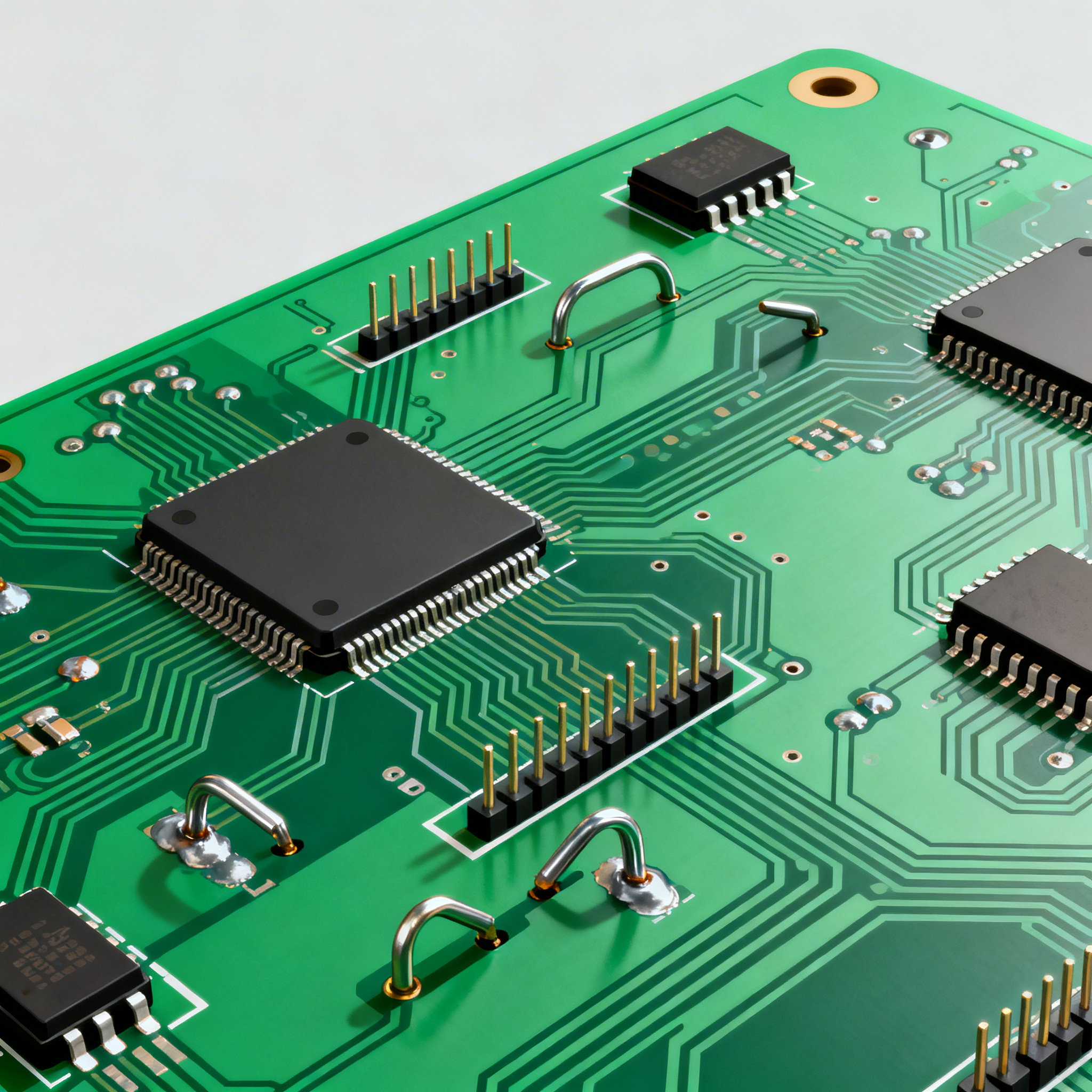
PCBs are essential in supporting and connecting various electronic components using conductive pathways. The design and manufacturing process of PCBs is complex, involving multiple layers of copper and dielectric materials. Key concepts include signal integrity, which ensures that signals are transmitted without distortion, and stack-up design, which involves arranging the layers of a PCB to optimize performance and minimize interference. Adhering to industry standards such as those from the IPC is critical for maintaining quality and reliability. These standards provide guidelines for trace width, spacing, via sizes, and more, which help in minimizing defects and enhancing the performance of the final product.
Detailed Specifications
When designing PCBs, several specifications need to be considered to ensure a successful layout and assembly. These include trace width, spacing, via sizes, and clearances, all of which are governed by IPC standards. Proper adherence to these specifications ensures signal integrity, reduces electromagnetic interference, and facilitates effective manufacturing processes. Understanding these specifications is crucial for both novice and experienced engineers to avoid common pitfalls and defects in PCB assembly.
| Design Rule | Minimum Value | Recommended Value |
|---|---|---|
| Trace Width | 0.1 mm | 0.2 mm |
| Trace Spacing | 0.1 mm | 0.2 mm |
| Via Diameter | 0.3 mm | 0.5 mm |
| Via Hole Size | 0.15 mm | 0.25 mm |
| Pad to Pad Clearance | 0.2 mm | 0.3 mm |
| Pad to Trace Clearance | 0.2 mm | 0.3 mm |
| Layer to Layer Clearance | 0.5 mm | 0.7 mm |
| Solder Mask Clearance | 0.05 mm | 0.1 mm |
| Solder Mask Dam | 0.1 mm | 0.15 mm |
| Silkscreen to Solder Mask Clearance | 0.1 mm | 0.2 mm |
Key Takeaways from the Specifications
The data presented in Table 1 highlights the critical design rules that engineers must adhere to when creating a PCB layout. Ensuring that trace widths and spacings are within the recommended values helps maintain signal integrity and reduces the risk of short circuits. Vias, which connect different layers of a PCB, must also be appropriately sized to ensure reliable connections without compromising the board's structural integrity. Clearances, both for pads and traces, are essential in preventing solder bridging during assembly. By following these guidelines, designers can minimize defects and enhance the overall performance of the PCB.
| Layer Configuration | Signal Layers | Power/Ground Layers |
|---|---|---|
| 2-Layer | 1 | 1 |
| 4-Layer | 2 | 2 |
| 6-Layer | 4 | 2 |
| 8-Layer | 6 | 2 |
| 10-Layer | 8 | 2 |
| 12-Layer | 8 | 4 |
| 14-Layer | 10 | 4 |
| 16-Layer | 12 | 4 |
Practical Implications
Table 2 provides insights into various layer stack-up configurations used in PCB design. The choice of layer configuration directly impacts the PCB's ability to handle complex circuitry and high-speed signals. For instance, a 4-layer board offers better signal integrity and reduced electromagnetic interference compared to a 2-layer board due to dedicated power and ground planes. As the number of layers increases, so does the complexity and cost. Therefore, selecting the appropriate stack-up is a balance between performance requirements and budget constraints. Understanding these configurations helps designers optimize their designs for specific applications, ensuring reliability and efficiency.
| Material | Dielectric Constant (Dk) | Loss Tangent (Df) |
|---|---|---|
| FR-4 | 4.5 | 0.02 |
| Rogers 4350B | 3.48 | 0.0037 |
| Rogers 4003C | 3.38 | 0.0027 |
| Polyimide | 4.2 | 0.004 |
| PTFE | 2.1 | 0.001 |
| Ceramic | 9.8 | 0.0005 |
| BT Epoxy | 4.2 | 0.015 |
| Arlon 85N | 3.5 | 0.003 |
| Nelco N7000 | 3.7 | 0.004 |
| Isola FR408HR | 3.66 | 0.009 |
Application Guidelines
Material selection is a critical aspect of PCB design, as it influences the board's electrical performance and thermal management. Table 3 offers a comparison of various materials, highlighting their dielectric constants and loss tangents. FR-4, being the most common material, offers a good balance of performance and cost. However, for high-frequency applications, materials like Rogers 4350B and PTFE are preferred due to their lower dielectric constants and loss tangents, which minimize signal loss. Understanding these properties helps in selecting the right material for specific applications, ensuring that the PCB meets performance requirements and operates reliably under varying conditions.
Design Considerations
When designing a PCB, several critical considerations must be taken into account to ensure optimal performance and manufacturability. Firstly, signal integrity must be maintained by minimizing crosstalk and reflections through proper trace routing and impedance matching. The stack-up design should be carefully chosen to provide adequate power distribution and ground planes, which help in reducing electromagnetic interference. Component placement is another vital aspect, as it affects thermal management and ease of assembly. Designers should also consider the manufacturability of the PCB, ensuring that design rules align with the capabilities of the fabrication and assembly processes. This involves selecting appropriate trace widths, via sizes, and clearances to avoid common defects such as solder bridging and open circuits. By adhering to these design considerations, engineers can create PCBs that are not only functional but also reliable and cost-effective.
Step-by-Step Implementation
Implementing a successful PCB design involves several key steps that ensure both functionality and manufacturability. Here's a detailed guide:
- Define Specifications: Begin by outlining the electrical and mechanical requirements, including size constraints, power levels, and signal types.
- Select Materials: Choose appropriate materials based on performance needs, considering factors such as dielectric constant and thermal properties.
- Design the Schematic: Create a detailed circuit schematic that includes all components and connections.
- Plan the Layout: Develop the PCB layout, paying close attention to trace routing, component placement, and layer stack-up.
- Simulate for Signal Integrity: Use simulation tools to analyze signal integrity, ensuring minimal loss and interference.
- Review and Optimize: Conduct a thorough design review to identify potential issues and optimize the layout for manufacturability.
- Generate Manufacturing Files: Prepare the necessary files, such as Gerber files, for fabrication and assembly.
- Prototype and Test: Fabricate a prototype board, conduct testing to verify functionality, and refine the design as needed.
By following these steps, designers can systematically tackle the complexities of PCB design, ensuring that the final product meets all specified requirements and is ready for mass production.
Common Issues & Solutions
PCB assembly often encounters several common issues, which can impact the board's functionality and reliability. Here are some typical problems and their solutions:
- Solder Bridging: Caused by excess solder or improper pad design, this can be mitigated by ensuring correct pad sizes and using solder masks.
- Open Circuits: Often due to incomplete solder joints, this issue can be resolved by optimizing reflow profiles and ensuring proper solder paste application.
- Component Misalignment: This can occur due to inaccurate placement or movement during soldering. Using precise pick-and-place machines and appropriate soldering techniques can help.
- Delamination: Caused by moisture absorption or thermal stress, delamination can be reduced by using high-quality materials and appropriate pre-baking processes.
- Electromagnetic Interference (EMI): Poor layout can lead to EMI issues, which can be minimized by proper grounding and shielding techniques.
- Thermal Issues: Inadequate thermal management can lead to overheating, which can be addressed by using thermal vias and heat sinks.
By understanding these common issues and their solutions, engineers can implement effective design and assembly practices that enhance the reliability and performance of PCBs.
Applications & Use Cases
PCBs are used in a wide range of applications across various industries. In consumer electronics, they are the backbone of devices such as smartphones, tablets, and laptops, providing the necessary circuitry for functionality. In the automotive industry, PCBs are used in engine control units, infotainment systems, and advanced driver-assistance systems (ADAS), where they must withstand harsh environmental conditions. In the medical field, PCBs are critical in diagnostic equipment and patient monitoring systems, where precision and reliability are paramount. The versatility and adaptability of PCBs make them indispensable in modern technology, driving innovation and efficiency across numerous sectors.
Selection & Sourcing Guide
Selecting the right components and materials for PCB design is crucial for ensuring performance and reliability. Engineers can leverage resources such as IC Online to source high-quality components and materials. This platform offers a comprehensive selection of electronic components, allowing designers to find the best options that meet their specific design requirements and budget constraints. By utilizing trusted sources, engineers can ensure that their PCBs are built with reliable and high-performance components.
FAQ
Here are some frequently asked questions regarding PCB design and assembly:
- What is the importance of trace width in PCB design? Trace width affects the current-carrying capacity and resistance of the PCB, impacting signal integrity and thermal management.
- How does layer stack-up affect PCB performance? The stack-up determines the distribution of signal, power, and ground layers, influencing signal integrity and electromagnetic interference.
- What materials are best for high-frequency applications? Materials with low dielectric constants and loss tangents, such as Rogers and PTFE, are ideal for high-frequency applications.
- How can I prevent solder bridging? Using appropriate pad sizes, solder masks, and controlled solder paste application can help prevent solder bridging.
- What is the role of thermal vias in PCB design? Thermal vias facilitate heat dissipation by providing a path for heat to transfer from hot components to cooler areas of the board.
- How can I ensure signal integrity in high-speed PCBs? Proper trace routing, impedance matching, and the use of ground planes are essential for maintaining signal integrity.
- What are the benefits of using simulation tools in PCB design? Simulation tools help identify potential signal integrity issues and optimize the design before fabrication, reducing the risk of defects.
- How do I choose the right PCB manufacturer? Consider factors such as manufacturing capabilities, quality standards, turnaround time, and cost when selecting a PCB manufacturer.
- What are the common causes of PCB delamination? Delamination is often caused by moisture absorption, thermal stress, or poor material quality.
- How can I improve the reliability of my PCB design? Following design guidelines, using high-quality materials, and conducting thorough testing can enhance the reliability of a PCB design.
Conclusion
In conclusion, understanding the intricacies of PCB design and assembly is essential for creating reliable and high-performance electronic devices. By adhering to industry standards, selecting appropriate materials, and following best practices in design and manufacturing, engineers can minimize defects and enhance the functionality of their PCBs. This article has provided insights into the critical design rules, layer stack-up options, and material properties that influence PCB performance, equipping designers with the knowledge to tackle the challenges of modern PCB design.
``` This article provides a comprehensive overview of PCB assembly defects, focusing on critical design and manufacturing considerations. It includes tables with detailed specifications, practical implications, and guidelines for real-world applications, all formatted in HTML.