Mastering Reflow Soldering Optimization for High-Density 4-Layer PCBs
Introduction In the fast-evolving electronics industry, mastering reflow soldering optimization for high-density 4-layer PCBs is crucial for engineers and manufacturers. As devices become more compact...
Introduction
In the fast-evolving electronics industry, mastering reflow soldering optimization for high-density 4-layer PCBs is crucial for engineers and manufacturers. As devices become more compact, the demand for high-density PCBs grows, necessitating a deep understanding of precise soldering techniques. Reflow soldering, a process that involves melting solder paste to establish electrical connections, is pivotal in achieving reliable and efficient PCB assemblies. This article explores the intricacies of optimizing reflow soldering for 4-layer PCBs, including layout rules, stackup design, signal integrity, and manufacturing considerations. Understanding these components ensures high-performance results, essential for modern electronics applications.
Technical Overview
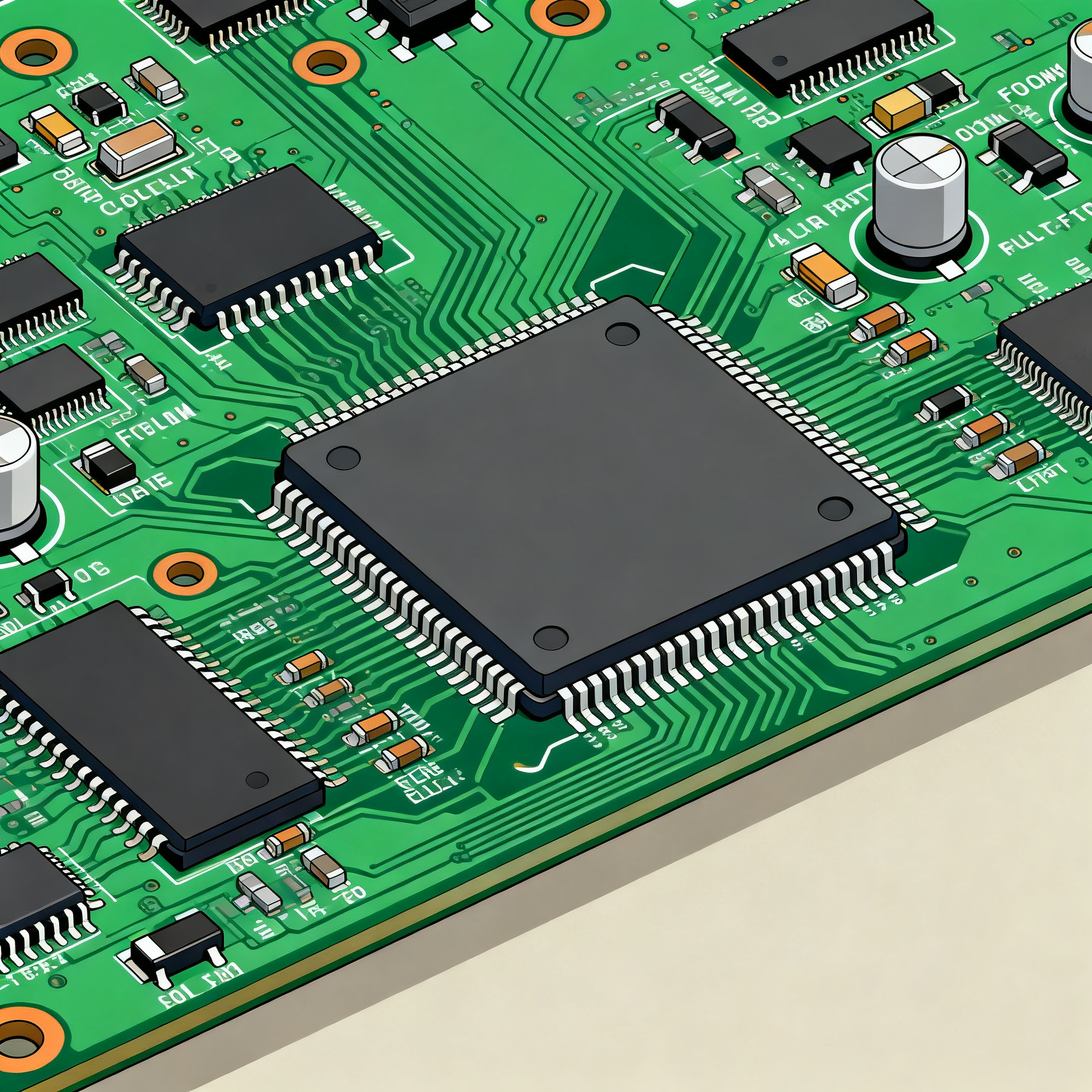
Reflow soldering is a critical process in PCB assembly that requires precise temperature control and timing. It involves applying solder paste to PCB pads, placing components, and then heating the assembly to melt the solder, creating durable connections. For high-density 4-layer PCBs, the complexity increases due to the need for precise control of thermal profiles and alignment of multilayer structures. The architecture of a 4-layer PCB typically includes a signal layer, a ground plane, a power plane, and another signal layer. This configuration supports better signal integrity and power distribution, essential for high-frequency applications. Key principles include maintaining appropriate trace widths and spacing, selecting suitable materials, and ensuring a balanced stackup design to minimize warping and signal loss.
Detailed Specifications
Specifications play a vital role in PCB design and manufacturing, dictating the parameters necessary for optimal performance. For high-density 4-layer PCBs, critical specifications include trace width, spacing, via sizes, and clearances. These parameters ensure that the PCB can handle the intended electrical loads without compromising signal integrity or causing shorts.
| Design Rule | Minimum Value | Recommended Value |
|---|---|---|
| Trace Width | 4 mils | 6 mils |
| Trace Spacing | 4 mils | 6 mils |
| Via Diameter | 8 mils | 10 mils |
| Annular Ring | 3 mils | 5 mils |
| Clearance to Edge | 10 mils | 20 mils |
| Pad to Trace Spacing | 4 mils | 6 mils |
| Drill Hole Size | 10 mils | 12 mils |
| Board Thickness | 0.8 mm | 1.6 mm |
| Aspect Ratio | 6:1 | 8:1 |
| Impedance Control | ±10% | ±5% |
Key Takeaways from the Specifications
The design rules outlined are critical for ensuring the reliability and functionality of high-density 4-layer PCBs. For instance, maintaining a minimum trace width of 4 mils helps prevent overheating and ensures adequate current flow. Similarly, appropriate trace spacing reduces the risk of short circuits and signal interference. The via diameter and annular ring sizes are essential for mechanical stability and electrical connectivity across layers. Understanding these specifications allows designers to optimize PCBs for performance and manufacturability, balancing cost with technical requirements.
| Layer Configuration | Signal Integrity | Thermal Management |
|---|---|---|
| Signal-Ground-Power-Signal | High | Moderate |
| Signal-Power-Ground-Signal | Moderate | High |
| Power-Signal-Ground-Signal | Moderate | Moderate |
| Ground-Signal-Power-Signal | High | Low |
| Signal-Ground-Signal-Power | High | Low |
| Signal-Power-Signal-Ground | Low | High |
| Power-Ground-Signal-Signal | Moderate | Moderate |
Practical Implications
The choice of layer stackup configuration significantly impacts signal integrity and thermal management. For example, a Signal-Ground-Power-Signal configuration offers high signal integrity due to dedicated ground and power planes, reducing electromagnetic interference (EMI). However, the thermal management in such configurations might be moderate. Conversely, a Signal-Power-Ground-Signal stackup provides better thermal management, making it suitable for power-intensive applications. Designers must weigh these factors based on the application's specific requirements, ensuring that the chosen stackup aligns with the performance and thermal needs of the PCB.
| Material | Dielectric Constant (Dk) | Loss Tangent (Df) |
|---|---|---|
| FR-4 | 4.5 | 0.020 |
| Rogers 4350B | 3.48 | 0.0037 |
| Rogers 4003C | 3.38 | 0.0027 |
| Isola FR408 | 3.75 | 0.009 |
| Nelco N4000-13 | 3.7 | 0.009 |
| Arlon 85N | 3.5 | 0.004 |
| Megtron 6 | 3.3 | 0.002 |
| Polyimide | 4.2 | 0.008 |
| PTFE | 2.2 | 0.001 |
Application Guidelines
Choosing the right material for a 4-layer PCB is critical for achieving desired electrical performance and reliability. FR-4 is a common choice due to its cost-effectiveness and adequate performance for many applications. However, for high-frequency applications, materials like Rogers 4350B or Megtron 6, with lower dielectric constants and loss tangents, are preferred to minimize signal loss. The dielectric constant affects the speed of signal propagation, while the loss tangent influences signal attenuation. Understanding these material properties helps in selecting the appropriate substrate, ensuring the PCB meets both performance and budgetary constraints.
Design Considerations
When designing high-density 4-layer PCBs, several considerations must be addressed to ensure optimal performance and manufacturability. First, ensure that the trace widths and spacing adhere to the design rules to prevent potential electrical issues. The choice of stackup configuration should align with the application's signal integrity and thermal management needs. Additionally, selecting the appropriate materials based on their dielectric properties can significantly impact the PCB's performance, particularly in high-frequency applications. Implementing impedance control is also vital for maintaining signal integrity, especially in RF and high-speed digital circuits. Designers should also consider manufacturability aspects, such as panelization and solder mask design, to facilitate efficient production and assembly.
Step-by-Step Implementation
- Define Requirements: Clearly outline the electrical, mechanical, and environmental requirements for the PCB.
- Select Materials: Choose the appropriate substrate and copper thickness based on performance needs and cost constraints.
- Design the Schematic: Develop a detailed schematic diagram ensuring all components and connections are correctly represented.
- Layout the PCB: Use PCB design software to layout the traces, vias, and components, adhering to design rules and stackup considerations.
- Simulate and Optimize: Perform signal integrity and thermal simulations to identify and resolve potential issues.
- Generate Gerber Files: Create Gerber files and other necessary documentation for manufacturing.
- Prototype and Test: Fabricate a prototype PCB and conduct thorough testing to validate design performance.
- Iterate and Finalize: Make necessary adjustments based on testing results and prepare the final design for mass production.
Common Issues & Solutions
- Issue: Solder Bridging - Solution: Optimize solder paste volume and stencil design.
- Issue: Warping - Solution: Use a balanced stackup design and appropriate materials.
- Issue: Signal Integrity Loss - Solution: Implement impedance control and use low-loss materials.
- Issue: Insufficient Thermal Management - Solution: Optimize layer configuration for better heat dissipation.
- Issue: Component Misalignment - Solution: Ensure accurate placement and alignment during assembly.
- Issue: Poor Via Reliability - Solution: Adhere to recommended via sizes and aspect ratios.
Applications & Use Cases
High-density 4-layer PCBs are prevalent in various applications, including consumer electronics, telecommunications, and automotive systems. In consumer electronics, they enable compact and efficient designs for smartphones and wearable devices. In telecommunications, they support high-speed data transmission in routers and switches. Automotive systems utilize these PCBs for advanced driver-assistance systems (ADAS) and infotainment systems, where reliability and performance are critical. The versatility and performance of 4-layer PCBs make them suitable for any application requiring complex circuitry and robust signal integrity.
Selection & Sourcing Guide
When selecting and sourcing materials and components for 4-layer PCBs, it's essential to consider both performance and cost. Utilize resources like IC Online to find reliable suppliers and compare options. Ensure that the chosen materials and components meet the technical specifications required for your design while offering competitive pricing. Engaging with experienced suppliers can also provide valuable insights and recommendations, enhancing the overall quality and reliability of your PCB assemblies.
FAQ
- What is a 4-layer PCB? A 4-layer PCB consists of four conductive layers, typically arranged as two signal layers, a power plane, and a ground plane, to enhance signal integrity and power distribution.
- Why use reflow soldering for PCBs? Reflow soldering offers precise control over solder joint formation, ensuring reliable and efficient connections in high-density assemblies.
- How do I choose the right stackup configuration? Consider the application's signal integrity and thermal management needs, selecting a stackup that balances these requirements.
- What materials are best for high-frequency applications? Materials like Rogers 4350B and Megtron 6, with low dielectric constants and loss tangents, are ideal for minimizing signal loss in high-frequency applications.
- How can I improve signal integrity in my PCB design? Implement impedance control, use low-loss materials, and optimize trace widths and spacing according to design rules.
- What are the common challenges in reflow soldering? Challenges include solder bridging, warping, and component misalignment, which can be mitigated through optimization of process parameters.
- What is impedance control? Impedance control involves designing traces with specific widths and spacing to maintain consistent impedance, crucial for signal integrity in RF and high-speed digital circuits.
- How do I ensure reliable via connections? Follow recommended via sizes and aspect ratios, and use suitable materials to enhance via reliability.
- Can I use FR-4 for all applications? While FR-4 is versatile and cost-effective, it may not be suitable for high-frequency applications requiring low-loss materials.
- How important is thermal management in PCB design? Thermal management is critical to prevent overheating and ensure the longevity and reliability of electronic components.
Conclusion
Mastering reflow soldering optimization for high-density 4-layer PCBs is essential for engineers and manufacturers seeking to achieve reliable and efficient PCB assemblies. By understanding and implementing design rules, stackup configurations, and material properties, designers can enhance signal integrity, thermal management, and overall performance. This comprehensive approach ensures that the resulting PCBs meet the demands of modern electronics applications, offering robust solutions for a wide range of industries.