Choosing High-Speed Materials for PCBs: The Engineer's Guide to 2026 Trends
Choosing High-Speed Materials for PCBs: The Engineer's Guide to 2026 Trends Introduction As we approach 2026, the world of high-speed printed circuit boards (PCBs) is rapidly evolving. The demand for ...
Introduction
As we approach 2026, the world of high-speed printed circuit boards (PCBs) is rapidly evolving. The demand for faster and more efficient electronic devices is driving engineers to explore new materials and design strategies. This guide delves into the trends shaping the choice of materials for high-speed PCBs, focusing on layout rules, stackup design, signal integrity, and manufacturing considerations. Understanding these elements is crucial for engineers aiming to optimize performance and reliability in their PCB designs.
Technical Overview
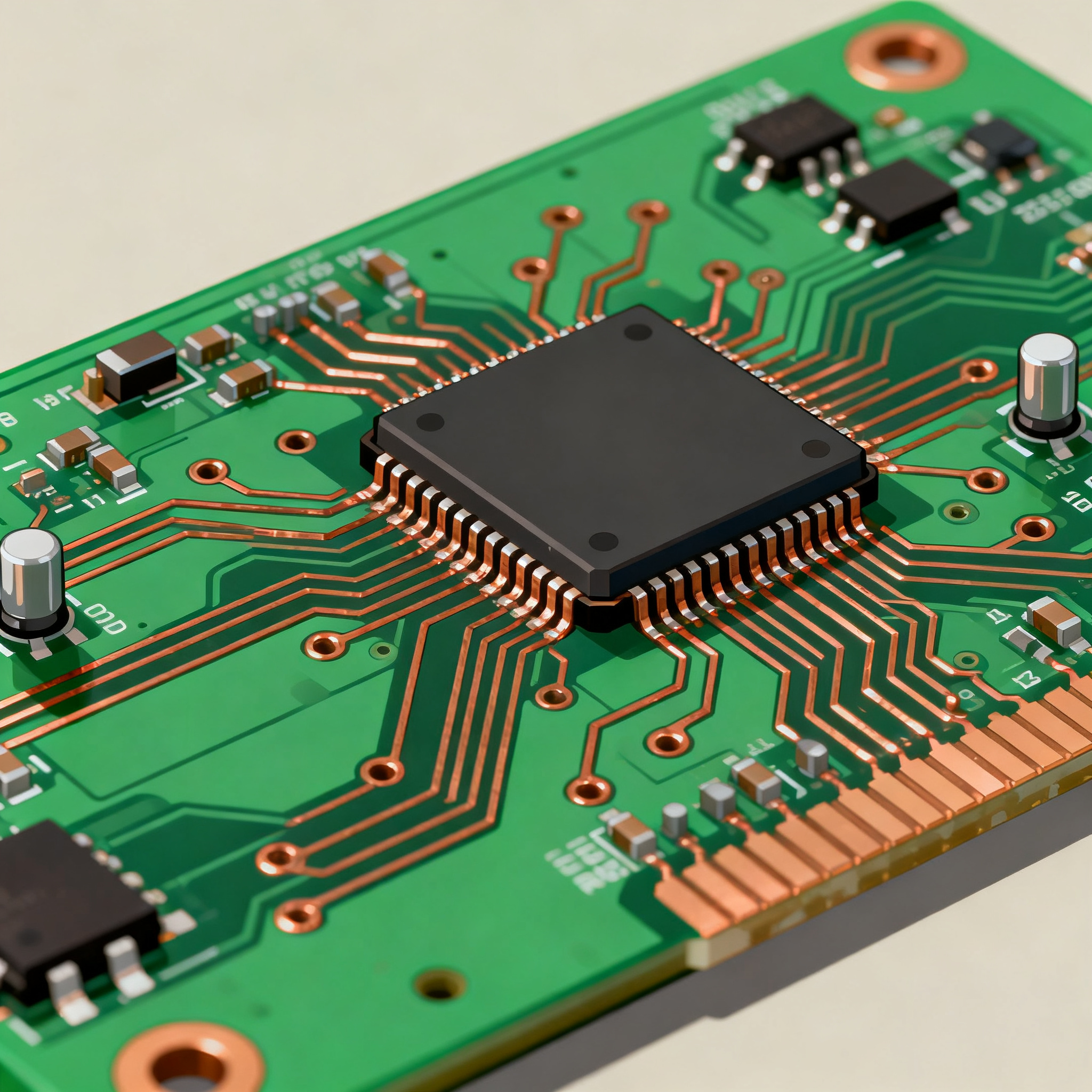
High-speed PCB design is a complex field that requires a thorough understanding of several core concepts. The architecture of a PCB involves multiple layers of conductive traces and insulating materials. The principles of signal integrity are paramount, as they ensure that signals are transmitted without degradation. This involves managing parameters like impedance, crosstalk, and electromagnetic interference (EMI). As technology advances, new materials with specific dielectric properties are being used to meet the demands of high-speed applications. These materials must be carefully selected and integrated into the PCB design to achieve the desired electrical performance.
Detailed Specifications
When designing high-speed PCBs, several specifications must be considered to ensure optimal performance. These include trace width, spacing, via sizes, and clearances. Each specification plays a critical role in maintaining signal integrity and ensuring reliable operation. The following table outlines key PCB design rules that engineers should follow when working with high-speed materials.
| Design Parameter | Recommended Value | Description |
|---|---|---|
| Trace Width | 4 mils | Minimum width for signal traces to maintain integrity |
| Trace Spacing | 4 mils | Minimum spacing between traces to prevent crosstalk |
| Via Diameter | 10 mils | Standard via size for reliable connections |
| Via Hole Size | 6 mils | Minimum hole size for through-hole connections |
| Clearance | 8 mils | Minimum clearance for electrical isolation |
| Impedance Control | 50 ohms | Standard impedance for high-speed signals |
| Layer-to-Layer Spacing | 5 mils | Minimum spacing to reduce crosstalk |
| Solder Mask Clearance | 3 mils | Minimum clearance for solder mask to avoid shorting |
| Drill to Copper | 8 mils | Minimum distance from drill hole to copper features |
| Annular Ring | 2 mils | Minimum ring width around vias for reliable soldering |
Key Takeaways from the Specifications
The specifications outlined in the table are critical for maintaining signal integrity in high-speed PCB designs. Trace width and spacing are particularly important as they directly influence impedance and crosstalk. Ensuring proper via sizes and clearances helps prevent manufacturing defects and electrical shorts. Adhering to these design rules is essential for achieving reliable and efficient high-speed PCBs. Engineers should always refer to the latest IPC standards and manufacturer guidelines to ensure compliance and optimal performance.
Layer Stackup Options
Layer stackup design is another crucial aspect of high-speed PCB design. It involves arranging the different layers of a PCB to optimize electrical performance and signal integrity. The following table presents various layer stackup configurations that are commonly used in high-speed PCB designs.
| Configuration | Layer Count | Typical Use |
|---|---|---|
| 2-Layer | 2 | Simple designs, low-cost applications |
| 4-Layer | 4 | Improved signal integrity, reduced EMI |
| 6-Layer | 6 | High-speed signals, better power distribution |
| 8-Layer | 8 | Complex designs, high-density interconnects |
| 10-Layer | 10 | Advanced applications, superior signal integrity |
| 12-Layer | 12 | Very high-speed applications, minimal crosstalk |
| 14-Layer | 14 | Ultra-high-speed, critical applications |
Practical Implications
Choosing the right layer stackup is essential for managing signal integrity and power distribution in high-speed PCBs. A higher layer count generally offers better performance by providing dedicated ground and power planes, which reduce EMI and crosstalk. However, it also increases the cost and complexity of the PCB. Engineers must balance these factors based on the specific requirements of their applications. For instance, a 4-layer stackup may suffice for moderate-speed applications, while more complex designs might necessitate a 10-layer or higher configuration.
Material Properties
The choice of materials is a critical factor in high-speed PCB design, affecting both electrical performance and manufacturability. Different materials offer varying dielectric constants and loss tangents, which influence signal propagation and attenuation. The table below compares common materials used in high-speed PCBs.
| Material | Dielectric Constant (Dk) | Loss Tangent (Df) |
|---|---|---|
| FR-4 | 4.5 | 0.020 |
| Rogers 4350B | 3.48 | 0.0037 |
| Rogers 4003C | 3.38 | 0.0027 |
| Isola IS620 | 3.45 | 0.0030 |
| Megtron 6 | 3.7 | 0.002 |
| Nelco N7000-2 | 3.4 | 0.0025 |
| Arlon 85N | 3.5 | 0.0035 |
| Panasonic R-5775 | 3.5 | 0.0025 |
| Taconic RF-35 | 3.5 | 0.0035 |
Application Guidelines
The material properties outlined in the table are crucial for selecting the right substrate for high-speed applications. Lower dielectric constants and loss tangents typically result in better high-frequency performance. For instance, Rogers materials are preferred for RF and microwave applications due to their superior electrical properties. FR-4, while cost-effective, may not be suitable for very high-speed designs due to its higher loss tangent. Engineers must evaluate the trade-offs between cost, performance, and manufacturing complexity when selecting materials for their PCBs.
Design Considerations
When designing high-speed PCBs, several practical guidelines must be followed to ensure optimal performance. First, maintaining consistent trace impedance is crucial for signal integrity. This can be achieved by carefully controlling trace width and spacing, as well as selecting the appropriate dielectric material. Second, minimizing the loop area for signal paths reduces EMI and crosstalk. This involves placing ground planes close to signal layers and using short, direct return paths. Third, via management is important to prevent signal reflections and losses. Designers should use blind or buried vias where possible and avoid unnecessary via transitions. Finally, proper thermal management is essential to prevent overheating and maintain reliability. This can be achieved by using thermal vias, heat sinks, and adequate copper thickness.
Step-by-Step Implementation
- Define the electrical requirements: Determine the necessary signal speeds, power levels, and environmental conditions for your PCB.
- Select the appropriate materials: Choose substrates with suitable dielectric properties based on your application's frequency requirements.
- Design the layer stackup: Configure the layers to optimize signal integrity and power distribution, considering factors like impedance and crosstalk.
- Apply design rules: Use the specifications outlined in the earlier table to guide trace width, spacing, and via sizes.
- Simulate the design: Use simulation tools to validate signal integrity and identify potential issues before fabrication.
- Review manufacturability: Ensure the design meets the capabilities of your chosen PCB manufacturer, considering factors like minimum trace widths and drilling capabilities.
- Create detailed documentation: Prepare comprehensive design files, including Gerber files and assembly drawings, for manufacturing.
- Prototype and test: Fabricate a prototype and conduct thorough testing to verify electrical performance and reliability.
Common Issues & Solutions
- Impedance Mismatch: Ensure consistent trace impedance by adhering to design rules and using simulation tools.
- Crosstalk: Minimize crosstalk by maintaining adequate spacing between traces and using ground planes.
- Signal Reflection: Use controlled impedance traces and proper termination techniques to prevent reflections.
- Thermal Management: Implement heat dissipation strategies such as thermal vias and heat sinks.
- Manufacturing Defects: Work closely with manufacturers to ensure design rules align with their capabilities.
- EMI: Reduce EMI by minimizing loop areas and using shielding techniques.
Applications & Use Cases
High-speed PCBs are integral to various industries and applications. In telecommunications, they enable high-frequency signal transmission for 5G networks. In consumer electronics, they support the high-speed data processing required in smartphones and tablets. Automotive applications use high-speed PCBs for advanced driver-assistance systems (ADAS) and infotainment systems. In aerospace and defense, they are crucial for radar and communication systems. Each application has unique requirements, making the choice of materials and design strategies critical for success.
Selection & Sourcing Guide
When selecting materials and components for high-speed PCBs, it is essential to work with reputable suppliers. IC Online provides a comprehensive resource for sourcing electronic components and materials, offering a wide range of products from trusted manufacturers. Engineers should consider factors such as lead time, cost, and supplier reliability when sourcing materials for their PCB projects.
FAQ
- What is the importance of dielectric constant in PCB materials? The dielectric constant affects signal speed and impedance, crucial for maintaining signal integrity.
- How does loss tangent impact high-speed PCBs? A lower loss tangent reduces signal attenuation, improving high-frequency performance.
- Why are layer stackups important in PCB design? Stackups optimize signal integrity and power distribution, reducing EMI and crosstalk.
- What are the benefits of using Rogers materials? Rogers materials offer superior electrical properties, ideal for RF and microwave applications.
- How can signal integrity be maintained in high-speed designs? Consistent trace impedance, proper termination, and minimizing crosstalk are key strategies.
- What role do vias play in PCB design? Vias provide inter-layer connections but can introduce losses and reflections if not managed properly.
- How do thermal considerations affect PCB reliability? Effective thermal management prevents overheating, ensuring long-term reliability and performance.
- What factors influence the choice of PCB materials? Frequency requirements, cost, manufacturability, and environmental conditions are key considerations.
- How can EMI be reduced in high-speed PCBs? Minimizing loop areas, using ground planes, and employing shielding techniques effectively reduce EMI.
- Why is prototyping important in PCB design? Prototyping allows for testing and validation, identifying potential issues before mass production.
Conclusion
As the demand for high-speed electronic devices continues to grow, selecting the right materials and design strategies for PCBs is more critical than ever. By understanding the key specifications, layer stackup options, and material properties, engineers can optimize their designs for performance and reliability. Staying informed about industry standards and leveraging resources like IC Online will ensure successful PCB projects in the ever-evolving landscape of high-speed electronics.