Budgeting for Innovation: A Detailed Cost Breakdown of PCB Prototypes for Your Next Project
Budgeting for Innovation: A Detailed Cost Breakdown of PCB Prototypes for Your Next Project Introduction In the fast-evolving world of electronics, staying ahead requires constant innovation. Printed ...
Introduction
In the fast-evolving world of electronics, staying ahead requires constant innovation. Printed Circuit Boards (PCBs) are the backbone of modern electronic devices, and prototyping them efficiently can make or break a project. Understanding the cost breakdown of PCB prototypes is crucial for budgeting and ensuring your project stays on track. This article delves into the key specifications, performance metrics, and application guidelines to help you make informed decisions.
Technical Overview
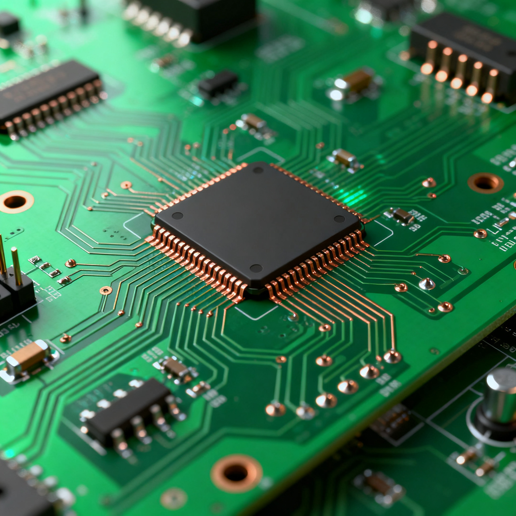
PCBs serve as the foundation for assembling electronic circuits. They mechanically support and electrically connect electronic components using conductive pathways, tracks, or signal traces etched from copper sheets laminated onto a non-conductive substrate. The design and manufacturing of PCBs are governed by standards such as IPC-A-610 and IPC-2221, which ensure quality and reliability. Understanding these principles is essential for designing PCBs that meet the desired performance and cost objectives.
The architecture of a PCB can vary from simple single-layer boards to complex multi-layer boards with advanced features like blind and buried vias. The choice of materials, layer count, and surface finish are critical factors that influence both the performance and the cost of the PCB. Additionally, the selection of components and the layout design play a significant role in the overall functionality and manufacturability of the PCB.
In this article, we will explore the detailed specifications that are crucial for PCB prototyping, examine the performance metrics that influence the design process, and provide an application matrix to guide you in selecting the right PCB configuration for your project.
Detailed Specifications
When designing a PCB prototype, understanding the key specifications is critical. These include parameters like layer count, material type, trace width, and surface finish. Each specification impacts the performance, manufacturability, and cost of the PCB. By analyzing these specifications, you can make informed decisions that align with your project's technical and budgetary requirements.
| Parameter | Specification | Importance |
|---|---|---|
| Layer Count | 1-16 Layers | Defines complexity and routing capability |
| Material | FR4, Rogers | Affects thermal and electrical performance |
| Trace Width | 3-10 mils | Impacts current carrying capacity |
| Surface Finish | HASL, ENIG | Determines solderability and shelf life |
| Board Thickness | 0.8-2.4 mm | Influences mechanical stability |
| Min. Hole Size | 0.2 mm | Affects via design and component placement |
| Min. Trace/Space | 3/3 mils | Determines routing density |
| Impedance Control | ±10% | Critical for high-frequency applications |
| Max. Board Size | 500 x 500 mm | Limits the design size |
| Copper Thickness | 1 oz, 2 oz | Impacts power handling capability |
| Solder Mask Color | Green, Blue, Black | Visual identification and aesthetics |
| Silkscreen | White, Yellow | Component labeling and identification |
Key Takeaways from the Specifications
The specifications outlined in the table above are fundamental to the design and functionality of a PCB. For instance, the layer count and material choice directly affect the board's complexity and performance in different environments. Selecting the right trace width and copper thickness ensures that the board can handle the necessary current loads without overheating. Additionally, surface finishes like HASL or ENIG play a crucial role in the solderability and longevity of the PCB. Understanding these specifications allows engineers to tailor their designs to meet specific application needs while maintaining cost-effectiveness.
| Metric | Value | Significance |
|---|---|---|
| Thermal Conductivity | 0.3 W/mK | Affects heat dissipation |
| Dielectric Constant | 4.2-4.5 | Influences signal integrity |
| Loss Tangent | 0.02 | Impacts high-frequency performance |
| CTE (X, Y, Z) | 17, 17, 70 ppm/°C | Determines thermal stability |
| Glass Transition Temp (Tg) | 130-170°C | Limits operational temperature |
| Peel Strength | 1.5 N/mm | Ensures mechanical reliability |
| Insulation Resistance | 10^9 Ω | Prevents leakage currents |
| Moisture Absorption | 0.10% | Affects dimensional stability |
| Flammability Rating | UL94 V-0 | Ensures safety standards |
| Surface Resistivity | 10^6 Ω/sq | Impacts electrical performance |
Practical Implications
The performance metrics detailed above provide insight into the electrical and thermal characteristics of the PCB materials. For example, thermal conductivity and CTE are critical for ensuring that the board can handle temperature variations without warping. The dielectric constant and loss tangent are essential for maintaining signal integrity, especially in high-frequency applications. Understanding these metrics helps in selecting the right materials and design parameters to ensure optimal performance and reliability of the PCB in its intended application.
| Use Case | Configuration | Benefits |
|---|---|---|
| Consumer Electronics | 4-layer, FR4, HASL | Cost-effective, reliable |
| Automotive | 6-layer, Rogers, ENIG | High thermal stability |
| Industrial Control | 8-layer, FR4, ENIG | Robust and durable |
| Telecommunications | 10-layer, Rogers, ENIG | Excellent signal integrity |
| Aerospace | 12-layer, High Tg, ENIG | Superior performance in extreme conditions |
| Medical Devices | 6-layer, FR4, ENIG | Biocompatible and reliable |
| Wearables | 2-layer, Flexible PCB, OSP | Lightweight and flexible |
| IoT Devices | 4-layer, FR4, HASL | Compact and efficient |
Application Guidelines
The application matrix provides a clear understanding of how different PCB configurations can be leveraged for specific use cases. For instance, consumer electronics benefit from a 4-layer FR4 design due to its cost-effectiveness, while automotive applications require the thermal stability offered by a 6-layer Rogers board. By matching the configuration to the application's demands, engineers can optimize performance and reliability while adhering to budget constraints. This approach ensures that the PCB design aligns with the end-use environment and operational requirements.
Design Considerations
Designing a PCB involves balancing numerous factors to achieve optimal performance and manufacturability. Here are some design considerations to keep in mind:
- Component Placement: Proper placement minimizes signal interference and optimizes thermal management. High-frequency components should be placed as close as possible to reduce trace lengths.
- Routing: Ensure that traces are routed efficiently to avoid signal integrity issues. Use wider traces for power and ground paths to reduce resistance and improve current flow.
- Via Design: Choose appropriate via types (through-hole, blind, or buried) based on layer count and routing needs. Consider via sizes and spacing to avoid manufacturing issues.
- Thermal Management: Incorporate thermal vias and heat sinks to dissipate heat effectively. Use thermal simulations to identify hotspots and optimize cooling strategies.
- Impedance Control: For high-speed designs, maintain controlled impedance by using appropriate trace widths and spacing. Use simulation tools to verify impedance matching.
- Design for Manufacturability (DFM): Follow IPC standards and manufacturer guidelines to ensure the design is manufacturable. Minimize complex features that may increase production costs.
- Testing and Validation: Design test points and include features for in-circuit testing to simplify validation and debugging processes.
By considering these factors during the design phase, you can create a PCB that meets performance requirements while remaining cost-effective and manufacturable.
Step-by-Step Implementation
Implementing a PCB design involves several critical steps. Here is a step-by-step guide to help you navigate the process:
- Define Requirements: Begin by defining the functional and performance requirements of the PCB. Understand the application and environment in which the PCB will operate.
- Component Selection: Choose components that meet the design specifications. Consider factors like availability, cost, and performance.
- Schematic Design: Create a schematic diagram that outlines the electrical connections between components. Use design software to ensure accuracy.
- PCB Layout: Translate the schematic into a physical PCB layout. Arrange components, route traces, and define layers to meet design constraints.
- Design Rule Check (DRC): Run a DRC to identify and resolve any layout issues. Ensure that the design complies with manufacturing and performance standards.
- Prototype Fabrication: Send the design to a PCB manufacturer for prototype fabrication. Choose a manufacturer that offers quick-turn services for faster iterations.
- Assembly and Testing: Assemble the prototype and conduct testing to validate performance. Identify and address any issues that arise during testing.
- Design Iteration: Based on test results, make necessary design adjustments. Iterate the process as needed to achieve the desired performance.
Following these steps ensures a structured approach to PCB design and implementation, allowing for efficient prototyping and validation.
Common Issues & Solutions
Designing and manufacturing PCBs can present several challenges. Here are some common issues and their solutions:
- Signal Integrity Issues: Use proper trace routing and impedance control to prevent signal degradation. Employ simulation tools to identify and address potential issues.
- Thermal Management Problems: Incorporate thermal vias and heat sinks to manage heat dissipation. Conduct thermal analysis to optimize cooling strategies.
- Manufacturing Defects: Follow IPC standards and perform thorough design rule checks to minimize defects. Choose a reputable manufacturer with quality control processes.
- Component Placement Errors: Ensure correct placement using design guidelines and simulation tools. Double-check component orientations and footprints.
- Power Distribution Challenges: Use wider traces for power and ground paths to reduce resistance. Consider adding decoupling capacitors for stable power supply.
- Design Complexity: Simplify the design by minimizing layer count and avoiding unnecessary features. Use modular design techniques to manage complexity.
By addressing these issues early in the design process, you can enhance the reliability and performance of the final PCB.
Applications & Use Cases
PCBs are used in a wide range of applications, each with unique requirements. Here are some notable use cases:
- Consumer Electronics: PCBs are integral to smartphones, tablets, and laptops, where compact size and cost-effectiveness are key.
- Automotive Electronics: Advanced driver-assistance systems (ADAS) and infotainment systems rely on PCBs for processing and connectivity.
- Medical Devices: PCBs are used in diagnostic equipment and wearable health monitors, where reliability and biocompatibility are crucial.
- Industrial Automation: PCBs enable control systems and robotics, providing durability and precision in harsh environments.
- Telecommunications: High-frequency PCBs are essential for network infrastructure, ensuring efficient data transmission.
Understanding the specific requirements of each application allows for tailored PCB designs that meet the demands of different industries.
Selection & Sourcing Guide
Selecting and sourcing the right components and PCBs is crucial for project success. Here are some tips:
- Utilize IC Online for component sourcing and availability checks.
- Collaborate with reputable PCB manufacturers like PCBWay and Nova PCBA for reliable fabrication and assembly services.
- Consider lead times, minimum order quantities (MOQs), and cost when selecting suppliers.
- Ensure that components and materials meet the necessary standards and certifications for your application.
By carefully selecting and sourcing components, you can ensure quality and reliability while optimizing costs.
FAQ
Here are some frequently asked questions about PCB prototyping:
- What is the typical lead time for PCB prototypes? Lead times can vary, but quick-turn services can deliver prototypes in as little as 3-5 days.
- How do I choose the right PCB material? Consider factors like thermal performance, dielectric constant, and cost. For high-frequency applications, materials like Rogers are preferred.
- What is the importance of impedance control? Impedance control is critical for maintaining signal integrity, especially in high-speed designs.
- How can I reduce the cost of PCB prototypes? Optimize design complexity, choose cost-effective materials, and consider higher MOQs for volume discounts.
- What are the common surface finishes for PCBs? Common finishes include HASL, ENIG, and OSP, each with specific benefits for solderability and shelf life.
- How do I ensure my PCB design is manufacturable? Follow IPC standards and design for manufacturability (DFM) guidelines to ensure the design can be produced efficiently.
- What tools are used for PCB design? Popular PCB design tools include Altium Designer, Eagle, and KiCad, offering features for schematic capture and layout design.
- How do I test a PCB prototype? Use in-circuit testing and functional testing to validate the performance and identify any issues.
- What is the role of a solder mask? The solder mask protects the PCB from oxidation and prevents solder bridges between components.
- How can I improve the thermal performance of a PCB? Use thermal vias, heat sinks, and thermal pads to enhance heat dissipation and prevent hotspots.
Conclusion
Budgeting for PCB prototypes involves understanding the detailed specifications, performance metrics, and application requirements. By considering these factors, you can design PCBs that meet your project's technical and budgetary goals. Leveraging the right tools, materials, and manufacturing partners ensures a successful prototyping process, paving the way for innovation and advancement in your electronic projects.