Wearable Device PCB Assembly Solutions
Struggling with reliable Wearable Device PCBA Solutions? NovaPCBA offers precision-focused assembly services tailored for wearables. Simplify your supply chain with our expertise in PCB fabrication, component sourcing, and advanced assembly techniques, ensuring high performance and quality.
Overview
Wearable Device PCBA Solutions — NovaPCBA's Specialized Service
Our Wearable Device PCBA Solutions are crafted for innovators in the wearable tech industry who demand precision and reliability. NovaPCBA excels in delivering advanced PCB assembly services, leveraging over 15 years of expertise. Adhering to IPC-A-610 standards, we address common challenges like miniaturization and connectivity, ensuring your wearable devices perform flawlessly in any condition.
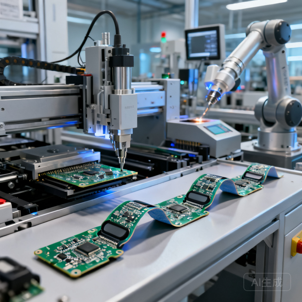
What's Included in Our Wearable Device PCBA Solutions
- Advanced SMT + THT Hybrid Assembly: We offer a combination of Surface Mount Technology (SMT) and Through-Hole Technology (THT) with Automated Optical Inspection (AOI) at every stage to ensure precision.
- Component Sourcing: Our extensive network guarantees high-quality components, reducing lead times and ensuring compatibility.
- Flexible & Rigid-Flex PCB Fabrication: We specialize in flexible and rigid-flex circuit designs, vital for compact and durable wearable devices.
- Box Build Assembly: Comprehensive services from PCB to final product assembly, simplifying your production process.
- Value-Added Processes: RoHS compliant soldering, conformal coating, and functional testing to ensure device reliability and longevity.
Industries & Applications
Our solutions cater to various industries, including healthcare, where precision in wearable medical devices is critical. The consumer electronics sector benefits from our expertise in smartwatches and fitness trackers, requiring robust and compact designs. Additionally, the sports industry leverages our solutions for performance monitoring devices, relying on durable and flexible PCB assemblies.
Our Manufacturing Process
- Design & Prototyping: Collaborate with our engineers to refine your design for manufacturability and performance.
- PCB Fabrication: Utilize our advanced facilities to produce high-quality PCBs tailored to your specifications.
- Assembly & Inspection: Implement SMT and THT techniques followed by exhaustive AOI and testing to ensure top quality.
- Final Testing & Packaging: Conduct thorough functional tests before packaging to guarantee reliability upon delivery.
Quality Assurance
Our quality assurance process adheres to IPC-A-610 Class 2/3 standards, employing AOI, X-ray inspections, and In-Circuit Testing (ICT) to capture solder joint defects, misplaced components, and connectivity issues. ISO9001 certification further ensures our commitment to delivering reliable products.
Frequently Asked Questions
- Q: How does NovaPCBA ensure the durability of wearable device PCBs?
- A: We use high-quality materials and advanced assembly techniques, including conformal coating and rigorous testing, to ensure durability and performance.
- Q: Can NovaPCBA handle low-volume, high-mix projects?
- A: Yes, we specialize in flexible production runs, accommodating both prototype and full-scale manufacturing needs.
- Q: What is the typical lead time for Wearable Device PCB Assembly Solutions?
- A: Typically, prototyping takes 2-4 weeks, while full production may range from 4-8 weeks depending on the complexity and volume.
Get a Quote for Wearable Device PCB Assembly Solutions
Contact us today with your Gerber files and BOM for a free quote. Benefit from our fast turnaround, expert engineering support, and unwavering commitment to quality at NovaPCBA.