UPS Power Module PCB Assembly
Ensure continuous power protection with our high-reliability UPS Power Module PCB Assembly. We specialize in advanced PCB assembly for UPS modules, delivering superior thermal management, precise component placement, and rigorous testing. Ideal for data centers, medical systems, and industrial backup power, our solutions guarantee performance when it matters most.
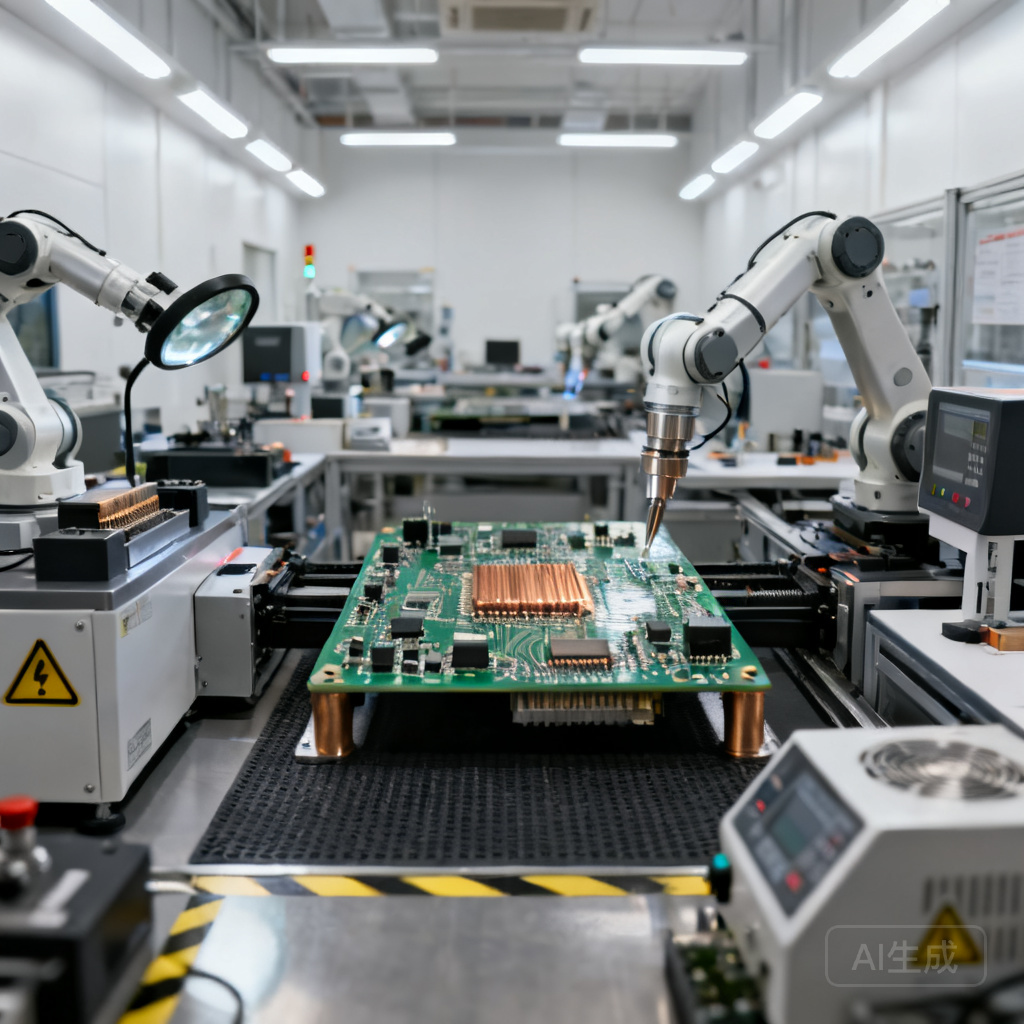
Overview
UPS Power Module PCB Assembly — NovaPCBA's Specialized Service
\nEvery power supply engineering team has felt the pain: a new UPS power module prototype fails during burn-in, or a production batch shows intermittent gate-drive faults that trace back to latent PCB defects. A 2026 industry report found that 62% of power supply NPI delays stem from suboptimal PCB layout for SiC/GaN circuits, while over 55% of high-power field failures originate from thermal imbalance and poor heat dissipation. Common failure modes—solder joint fatigue, voiding, delamination—are well documented in PCBA failure analysis guides. NovaPCBA's UPS Power Module PCB Assembly service is built to remove these risks. As a one-stop partner, similar to the model described by power supply PCBA specialists, we combine in-house heavy-copper fabrication, hybrid SMT/THT assembly, and rigorous inspection to deliver power modules that work first time—whether you are prototyping a 3 kW online UPS or ramping a 300 kVA modular system.
\n\nWhat's Included in Our UPS Power Module PCB Assembly Service
\n- \n
- Hybrid SMT + THT assembly with multi-stage AOI: Surface-mount components (MOSFETs, gate drivers, passives) are placed and reflowed, then through-hole power connectors, transformers, and bus bars are wave or selectively soldered. Automated optical inspection is performed after each soldering step, catching misalignment, bridging, and tombstoning before they propagate. \n
- Heavy copper up to 6 oz and metal-core substrates: High-current paths for battery charging and inverter stages are routed on thick copper layers to minimize I²R losses and temperature rise. We use proprietary sequential lamination and symmetric stack-up techniques that eliminate assembly-level warpage, ensuring flatness for heat sink contact. \n
- Controlled impedance for SiC/GaN gate-drive circuits: Fast-switching wide-bandgap devices demand precise impedance control on gate traces to prevent ringing and false turn-on. Our DFM review calculates trace geometry and dielectric spacing per IPC-2141, verified with TDR testing on first articles. \n
- Microprocessor-controlled logic assembly and firmware-ready testing: The control PCBA is assembled to the same Class 3 standard, with firmware flashing and basic functional checks available. This aligns with technical guide specifications that require all UPS operations to be firmware-controlled and self-diagnostic. \n
- Conformal coating and ruggedization: For UPS modules deployed in humid or dusty environments, we apply acrylic, silicone, or parylene coatings to protect against leakage currents and corrosion. \n
Industries & Applications
\nUPS power modules are mission-critical in environments where even a half-cycle interruption is unacceptable. Our PCB assemblies support:
\n- \n
- Data center and telecom UPS: Online double-conversion modules that continuously condition power. These boards must handle sustained high currents and 24/7 thermal cycling without degradation. \n
- Medical UPS systems: Equipment such as MRI scanners and life-support systems require PCBA with zero-delay transfer and galvanic isolation, built to IPC-A-610 Class 3 for patient safety. \n
- Industrial automation and motor drives: UPS modules that correct voltage sags and spikes using specialized inverter topologies, as detailed in UPS inverter design resources. These often require high-voltage clearance and robust thermal management. \n
- Renewable energy storage inverters: High-power modules up to 300 kVA, similar to the Salicru ADAPT series, that interface battery banks with the grid. Heavy copper and laminated bus structures are standard to handle the DC link. \n
Comparing Assembly Approaches for UPS Power Modules
\nChoosing the right manufacturing strategy directly impacts yield, lead time, and field reliability. The table below contrasts three common models.
\n| Factor | \nIn-House Assembly (NovaPCBA) | \nOffshore-Only Assembly | \nTurnkey (Consigned) | \n
|---|---|---|---|
| Lead Time | \n10–15 working days for prototypes; 4–6 weeks for production. No logistics lag. | \n6–10 weeks plus sea/air freight; customs delays common. Example: offshore UPS PCB suppliers often quote 8+ weeks. | \n3–5 weeks after component kit arrival, but kit-check and shortage handling add hidden time. | \n
| Defect Catch | \nAOI after each SMT/THT step, X-ray, ICT, and functional test per IPC-A-610 Class 3. Defects caught at the earliest stage. | \nOften limited to final AOI; no in-line SPI or post-wave AOI. Latent defects may escape to field. | \nDepends on partner capability. Without enforced multi-stage inspection, defect escape rates rise. | \n
| Cost Driver | \nHigher NRE but lower rework risk and zero hidden logistics fees. Total cost of ownership is optimized. | \nLow labor cost, but tariffs, shipping, and rework/returns erode savings. Communication overhead adds engineering time. | \nComponent procurement and supplier management dominate, as explained in a consigned PCBA cost guide. Shortage handling and rework risk increase final cost. | \n
| Failure Boundary | \nFull traceability, direct engineering feedback, and root cause analysis within days. Design issues fixed before production. | \nCommunication gaps delay failure analysis. Thermal imbalance and poor heat dissipation—cited in 55% of field failures—may go unresolved. | \nShared responsibility blurs accountability. Failure analysis can stall while supplier and customer exchange data. | \n
Our Manufacturing Process
\n- \n
- DFM and thermal simulation review: We analyze your Gerber files for creepage/clearance per IEC 62368-1, thermal relief on high-current nets, and impedance profiles for gate-drive loops. Recommendations are provided before fabrication to avoid the 62% NPI delay trap. \n
- SMT assembly with SPI and reflow profiling: Solder paste inspection checks volume and alignment before placement. Reflow ovens are profiled specifically for heavy copper boards to ensure complete wetting without overheating sensitive SiC/GaN devices. \n
- THT wave/selective soldering and press-fit: Large connectors, relays, and bus bars are assembled with controlled wave height or selective soldering. Press-fit pins are used where thermal stress must be avoided. \n
- ICT, functional test, and burn-in: In-circuit test verifies component values and polarity. Functional test applies actual UPS load profiles—battery charge, inverter output, static bypass—while monitoring temperature and waveforms. Burn-in cycling detects early-life failures. \n
Quality Assurance
\nEvery UPS power module PCB assembly is inspected to IPC-A-610 Class 2 or Class 3 acceptance criteria, as specified by the customer. Our multi-stage inspection regime catches defects that single-point checks miss:
\n- \n
- Automated Optical Inspection (AOI): Post-print, post-placement, and post-reflow AOI scans for solder bridging, insufficient solder, missing components, and lifted leads. Advanced algorithms, similar to the machine-learning systems described by AI-driven inspection providers, flag microscopic anomalies invisible to the human eye. \n
- X-ray inspection: BGA, QFN, and heavy copper thermal pad voiding are analyzed per IPC-7095. We reject boards with voiding >25% on power device pads, a common root cause of thermal runaway documented in failure analysis studies. \n
- In-Circuit Test (ICT) and Functional Test: ICT verifies resistance, capacitance, and diode polarity. Functional test simulates UPS modes—mains present, battery discharge, bypass—and measures output regulation, transient response, and efficiency. Only boards that pass full functional test under load are shipped. \n
Our facility operates under ISO9001:2015 quality management and complies with RoHS directives. All processes are documented and traceable to individual operator and machine logs.
\n\nFrequently Asked Questions
\n- \n
- Q: How do you ensure traceability and provide Certificates of Conformance (CoC) for critical UPS components? \n
- A: We maintain full batch traceability from component procurement through final test. Every reel and tube is logged with date code and supplier lot. Upon shipment, you receive a CoC listing the serial numbers, test results, and material declarations per RoHS/REACH. For safety-critical parts like isolation transformers or DC-link capacitors, we can provide additional supplier CoCs. \n
- Q: What should I look for when auditing a supplier for UPS Power Module PCB Assembly? \n
- A: Verify that the supplier has in-house heavy copper capability (≥4 oz), documented IPC-A-610 Class 3 workmanship, and multi-stage inspection (AOI, X-ray, ICT). Ask to see a process control plan for thermal management—how they prevent warpage and ensure heat sink flatness. Review their NPI process: a robust DFM check should catch layout issues that cause 62% of power supply NPI delays. Finally, confirm they have experience with UPS-specific tests like battery charge/discharge cycling and static bypass transfer. \n
- Q: What is the typical lead time for UPS Power Module PCB Assembly? \n
- A: Prototype builds of 5–50 units usually ship in 10–15 working days after Gerber approval and component availability. We can accelerate using reference designs, such as the ST UPS evaluation board, if you need a quick proof-of-concept. Production volumes of 500+ units ship in 4–6 weeks, supported by strategic safety stock of common high-power laminates and authorized distributor agreements that stabilize lead times, as recommended by supply chain best practices. \n
Get a Quote for UPS Power Module PCB Assembly
\nReady to move your UPS power module from concept to reliable production? Send your Gerber files, BOM, and any test specifications to our engineering team for a free, no-obligation quote. We respond within one business day with a detailed DFM review and lead time estimate. Let NovaPCBA's UPS Power Module PCB Assembly service be the foundation of your next high-reliability power system.
\n\n