Telecom Integrated Systems PCB Assembly Solutions
Transform your telecom systems with NovaPCBA's Telecom Integrated Systems PCB Assembly Solutions. Our ISO9001 and IPC-A-610 certified services address the industry's complex demands, ensuring seamless connectivity and reliability. Experience reduced downtime and enhanced performance with our tailored solutions.
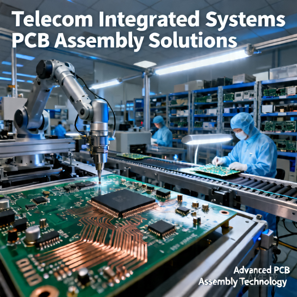
Overview
Telecom Integrated Systems PCB Assembly Solutions — NovaPCBA's Specialized Service
NovaPCBA offers Telecom Integrated Systems PCB Assembly Solutions designed for the telecommunication sector's dynamic needs. Our service is essential for companies requiring robust, high-performance PCB assemblies that comply with industry standards such as IPC-A-610. With over 15 years of experience, we understand the challenges of ensuring signal integrity and minimizing latency. Our approach focuses on precision, reliability, and flexibility, setting us apart from competitors.
What's Included in Our Telecom Integrated Systems PCB Assembly Solutions
- Hybrid Assembly: SMT + THT hybrid assembly with AOI inspection at every stage to ensure high precision and reliability.
- Component Procurement: Comprehensive sourcing and procurement of high-quality components to meet specific design requirements.
- Turnkey Solutions: Complete turnkey assembly including design, prototyping, and full-scale production.
- Testing and Validation: Extensive testing including ICT, functional testing, and X-ray inspection to guarantee performance and durability.
- Custom Design Support: Engineering support for custom designs to address unique application challenges.
Industries & Applications
Our Telecom Integrated Systems PCB Assembly Solutions are crucial for industries such as data centers, where high-speed data transfer and uninterrupted connectivity are paramount. Telecommunication network infrastructure relies on our solutions for reliable signal processing and routing. Additionally, the aerospace sector uses our assemblies in satellite communication systems, requiring robust and high-frequency performance.
Our Manufacturing Process
- Design Review: Comprehensive review of Gerber files and BOMs to ensure design feasibility and compliance with standards.
- Prototyping: Rapid prototyping to test and validate designs before full-scale production.
- Assembly: Precision assembly using state-of-the-art SMT and THT equipment.
- Testing: Rigorous testing including AOI, X-ray, and functional testing to ensure product quality and reliability.
Quality Assurance
Our quality assurance process adheres to IPC-A-610 Class 2/3 standards, involving AOI to detect misalignment and solder defects, X-ray for hidden solder joint inspection, and ICT for electrical functionality. Our ISO9001 certification guarantees a consistent, high-quality manufacturing process, and RoHS compliance ensures environmentally friendly products.
Frequently Asked Questions
- Q: How does NovaPCBA ensure signal integrity in their assemblies?
- A: We utilize advanced design techniques and testing protocols to maintain signal integrity, including impedance control and thorough RF testing.
- Q: Can NovaPCBA handle high-volume production?
- A: Yes, we are equipped to manage both low and high-volume production runs with consistent quality and efficiency.
- Q: What is the typical lead time for Telecom Integrated Systems PCB Assembly Solutions?
- A: Prototyping typically takes 2-3 weeks, while production runs depend on volume but generally range from 4-8 weeks.
Get a Quote for Telecom Integrated Systems PCB Assembly Solutions
Ready to enhance your telecom systems? Submit your Gerber files and BOM for a free quote today. Benefit from fast turnaround times, expert engineering support, and NovaPCBA's unwavering commitment to quality. Contact us now to start your project.