Smart Utility Meter PCB Assembly
At NovaPCBA, our Smart Utility Meter PCB Assembly services deliver precision-engineered boards for reliable energy monitoring. We ensure high-yield SMT assembly, rigorous testing, and robust connectivity for gas, water, and electricity meters, empowering utilities with accurate data collection and long-term performance in demanding environments.
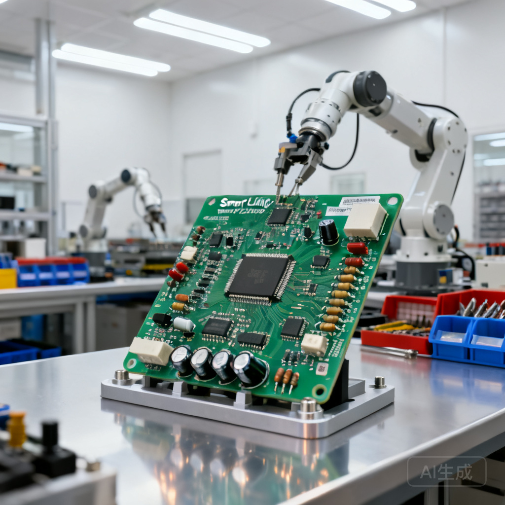
Overview
Smart Utility Meter PCB Assembly — NovaPCBA's Specialized Service
When a single batch of utility meter PCBs suffers from latent soldering defects, the result isn’t just a rework line stoppage — it’s a potential recall spanning thousands of installed units. As highlighted by the importance of device history records (DHR) in limiting recall scope (Best PCBs), undetected flaws like insufficient solder or misaligned components can cascade into field failures. For AMI system integrators and energy providers, yield loss discovered only after deployment is unacceptable. NovaPCBA’s Smart Utility Meter PCB Assembly service eliminates this risk with an ISO9001/IPC-A-610 certified process built on multi-stage automated optical inspection (AOI) at 5 µm resolution (AllPCB), precision impedance control for RF communication, and rigorous traceability from bare board to final test.
What's Included in Our Smart Utility Meter PCB Assembly
- SMT + Through-Hole Hybrid Assembly: Full turnkey assembly supporting 0201 passives, fine-pitch QFNs, and large connectors on the same board, with selective soldering for high-reliability through-hole components like shunt resistors and transformers. (TopfastPCB)
- Impedance-Controlled RF Layout: Stackup design and controlled dielectric processing for sub-1 GHz (868/915 MHz) and 2.4 GHz wireless meshes, ensuring consistent signal integrity for Zigbee, Wi-SUN, and cellular AMI modules.
- Ultra-Precise Analog Front-End Assembly: Specialized soldering techniques and board layout support for current shunts and voltage dividers that enable Class 0.1 and Class 0.2 metrology accuracy per IEC 62053. (FS PCBA)
- Conformal Coating & Potting: Selective conformal coating (acrylic, silicone, or parylene) and optional potting for outdoor meters exposed to humidity, dust, and temperature extremes, preventing dendritic growth and leakage currents.
- End-of-Line Functional Test Development: Custom test jigs that simulate AMI network communication, metrology calibration pulses, and tamper detection, verifying full board functionality before shipment.
Industries & Applications
Our Smart Utility Meter PCB Assembly serves the exacting demands of three core segments. Advanced Metering Infrastructure (AMI) providers rely on our assembly for residential and C&I smart meters where wireless mesh networking and long battery life require low-power SMT designs and zero-defect soldering. Grid automation OEMs use our boards in feeder automation controllers and fault passage indicators, demanding extended temperature range components and robust conformal coating. Sub-metering and energy management companies depend on our high-precision analog front-end assembly for multi-circuit energy monitors that must maintain Class 0.5 accuracy over a 10+ year service life, with full traceability to individual component lots.
Our Manufacturing Process
- DFM Review & Material Verification: Every BOM is checked against IEC 62053 and IPC-7351 footprints. We verify component availability and authenticity, and confirm PCB laminate (typically high-Tg FR-4 or polyimide for extended temperature) meets thermal requirements.
- SMT Assembly & In-Line AOI: Solder paste inspection (SPI) followed by high-speed placement and reflow. AOI systems scan every joint at 5 µm resolution immediately after reflow, flagging misalignment, insufficient solder, or tombstoning before the board leaves the line. (AllPCB)
- Through-Hole & Selective Soldering: Heavy-current shunts, terminal blocks, and transformers are inserted and soldered using selective wave or robotic soldering to avoid thermal shock to SMT components, with 100% visual inspection of each joint.
- Conformal Coating, Functional Test & DHR Compilation: Boards are coated, then subjected to ICT and functional test that verifies metrology accuracy, RF performance, and tamper detection. A complete device history record (DHR) is compiled, linking serial numbers to component lots, process parameters, and inspection results for rapid field recall containment. (Best PCBs)
In-House Assembly vs. Offshore-Only vs. Turnkey — A Comparison
| Factor | In-House Assembly (NovaPCBA) | Offshore-Only Provider | Turnkey Broker |
|---|---|---|---|
| Typical Lead Time | 10–15 working days for prototypes, 3–4 weeks for production volumes, with direct engineering communication. | 4–8 weeks (including shipping and customs), often with language barriers and time-zone delays. (TopfastPCB) | Variable; depends on subcontracted factory loading, often 5–7 weeks with limited visibility. |
| Defect Catch Rate | Multi-stage AOI (5 µm resolution) + X-ray + ICT. Defects like insufficient solder on QFN thermal pads are caught in-line, not at final test. | May rely on a single post-reflow AOI or sample-based inspection; higher risk of latent field failures escaping. (Best PCBA Manufacturer) | Inspection quality is factory-dependent; no unified process control, often missing AOI programming for fine-pitch metrology ICs. |
| Cost Driver | Moderate NRE offset by zero rework/recall risk and faster time-to-market. Total cost of ownership is lower for medium-to-high volumes. | Lower unit price, but hidden costs from scrap, rework, and field returns can exceed 15–20% of program cost. | Markup on subcontracted assembly; engineering changes incur additional charges and delays. |
| Failure Boundary | Full traceability via DHR; if a field issue occurs, affected units are identified by serial number in hours, not weeks. (Best PCBs) | Batch-level traceability only; a single failed unit can trigger a recall of an entire shipment. | Traceability limited to the broker’s paperwork; root cause analysis is slow and often inconclusive. |
Quality Assurance
Every Smart Utility Meter PCB Assembly undergoes a defense-in-depth inspection regimen aligned to IPC-A-610 Class 2 (residential meters) or Class 3 (critical grid infrastructure). Post-print solder paste inspection verifies deposit volume and alignment. In-line AOI at 5 µm resolution catches misaligned 0201 capacitors, insufficient solder on RF shields, and lifted leads before the board enters reflow. (AllPCB) X-ray inspection validates hidden joints under BGAs and QFNs, especially on wireless SoCs. In-circuit test (ICT) checks passive values, shorts, and opens. Finally, a custom functional test simulates real AMI network traffic, metrology calibration pulses, and tamper switch actuation, ensuring the board meets IEC 62053 accuracy limits. All process data is compiled into a serialized DHR, enabling precise lot containment in the unlikely event of a field return. We are ISO9001 certified and all assemblies are RoHS compliant; no other certifications are claimed beyond these verifiable standards.
Frequently Asked Questions
- Q: How do you audit and qualify a supplier for smart meter PCB assembly?
- A: We evaluate process capability, not just paperwork. Key checks include: AOI resolution and programming for metrology ICs, X-ray availability for hidden joints, impedance control test coupons, and a live DHR traceability demonstration. We also verify that the supplier’s solder profiles align with the thermal mass of shunt resistors and transformers used in Class 0.1/0.2 meters, referencing IPC-7530 guidelines.
- Q: What traceability and Certificate of Conformance (CoC) do you provide with each batch?
- A: Every shipment includes a CoC listing the IPC-A-610 class, RoHS compliance, and a summary of test results. We also deliver a full digital DHR package that links each PCB serial number to the component date/lot codes, solder paste batch, reflow profile, AOI images, and functional test pass/fail logs. This granularity enables rapid root cause analysis and limits any potential recall to the smallest possible subset.
- Q: What is the typical lead time for Smart Utility Meter PCB Assembly?
- A: For prototype builds (10–50 units), we deliver in 10–15 working days after BOM and Gerber approval. Production volumes of 1,000–10,000 units typically ship in 3–4 weeks. Rush services are available for critical grid rollout schedules; contact our engineering team with your specific timeline.
Get a Quote for Smart Utility Meter PCB Assembly
Submit your Gerber files and BOM for a free, no-obligation quote. Our engineers will review your design for metrology accuracy, RF impedance, and manufacturability, and provide a lead time within one business day. Rely on NovaPCBA’s ISO9001-certified facility to deliver utility-grade PCBs that pass field audits the first time.
References & Further Reading
- Smart Meter PCB Assembly & Manufacturing | TopfastPCB
- Smart Meter PCB Assembly: A Step-by-Step Guide | AllPCB
- Smart Meter PCB Manufacturing | TopfastPCB
- PCBA Blog – EBest Technology
- The Smart Choice: Understanding Smart Meter PCB Assembly | Best PCBA Manufacturer
- Energy Meter PCB: Types, Components, Design | FS PCBA