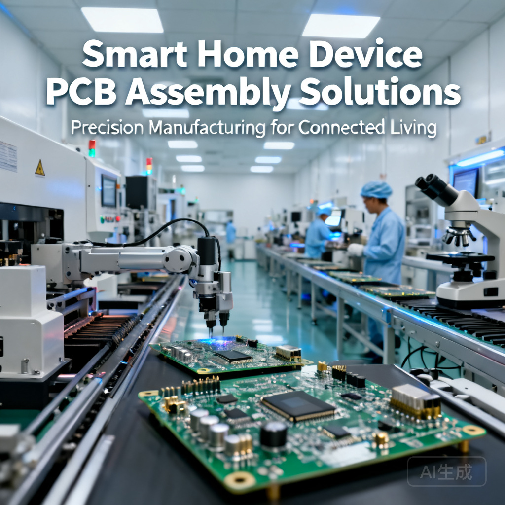
Smart Home Device PCB Assembly Solutions
Discover unparalleled Smart Home Device PCBA Solutions with NovaPCBA. We address complex design and assembly challenges, ensuring your smart home devices operate flawlessly. Leveraging 15+ years of expertise, we optimize your PCB assembly for the IoT era, enhancing reliability and performance in every home.
Overview
Smart Home Device PCBA Solutions — NovaPCBA's Specialized Service
In the rapidly evolving smart home market, reliable PCB assembly is critical for seamless device integration. NovaPCBA's Smart Home Device PCBA Solutions cater to manufacturers seeking precision and efficiency. Our ISO9001 and IPC-A-610 certified services ensure compliance with stringent industry standards, addressing common challenges such as miniaturization and multi-layered designs. Our experienced engineers employ cutting-edge techniques to enhance device performance and longevity.
What's Included in Our Smart Home Device PCBA Solutions
- Advanced Assembly Techniques: SMT + THT hybrid assembly with AOI inspection at every stage ensures optimal functionality.
- Design Optimization: We refine PCB layouts to accommodate IoT connectivity and power efficiency.
- Material Sourcing: Use of RoHS-compliant components guarantees environmental safety.
- Prototyping Services: Rapid prototyping to streamline design iterations and accelerate development.
- Custom Testing: Tailored functional testing to verify device-specific requirements and performance.
Industries & Applications
Our Smart Home Device PCBA Solutions serve industries such as home automation, where precise control systems are critical; consumer electronics, demanding compact and efficient PCBs; and energy management devices, requiring robust power handling capabilities. Each application benefits from our ability to produce high-quality, reliable assemblies aligned with industry standards.
Our Manufacturing Process
- Design Analysis: Initial assessment of PCB designs for manufacturability and performance optimization.
- Component Sourcing: Secure procurement of certified components to meet design specifications.
- Assembly: Precise assembly using SMT and THT processes, ensuring structural integrity.
- Testing and Inspection: Comprehensive testing including AOI, X-ray, and functional testing to confirm product quality.
Quality Assurance
Our QA process adheres to IPC-A-610 Class 2/3 standards, featuring automated optical inspection (AOI) to detect solder defects, X-ray inspection for hidden joint verification, and in-circuit testing (ICT) for electrical integrity. Our ISO9001 certification underlines our commitment to consistent quality and reliability in every assembly.
Frequently Asked Questions
- Q: How do you ensure compatibility with various smart home systems?
- A: We customize PCBA solutions to meet specific protocol and connectivity requirements, ensuring seamless integration with existing smart home infrastructure.
- Q: What is your approach to minimizing electromagnetic interference (EMI)?
- A: Our design optimization includes EMI shielding and strategic component placement to reduce interference and improve signal integrity.
- Q: What is the typical lead time for Smart Home Device PCB Assembly Solutions?
- A: Prototype assemblies are typically delivered within 2-3 weeks, while full production runs can be completed in 4-6 weeks, depending on complexity.
Get a Quote for Smart Home Device PCB Assembly Solutions
Ready to elevate your smart home devices? Submit your Gerber files and BOM for a free quote today. Experience fast turnaround, comprehensive engineering support, and NovaPCBA's unwavering commitment to quality.