Semiconductor Test Interface PCB Assembly
Precision-engineered Semiconductor Test Interface PCB Assembly ensures reliable wafer-level and package testing with high signal integrity and minimal insertion loss. At NovaPCBA, we deliver advanced interconnect solutions featuring tight impedance control and robust materials, enabling accurate device characterization and faster yield ramp for your most demanding semiconductor applications.
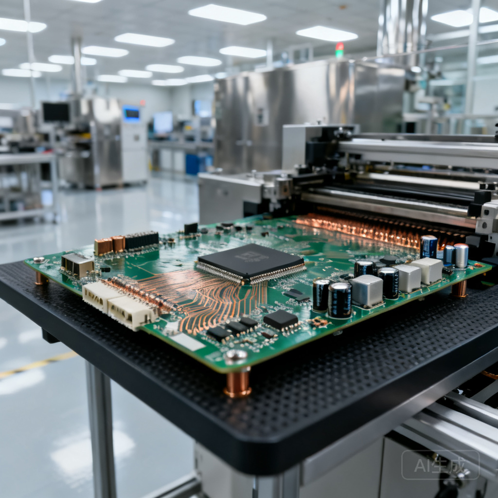
Overview
Semiconductor Test Interface PCB Assembly — NovaPCBA's Specialized Service
When a single impedance discontinuity on an ATE load board forces you to scrap an entire wafer-lot validation cycle, the cost isn't measured in board rework — it's measured in delayed tape-outs and lost fab capacity. Semiconductor test interface PCB assembly demands tolerances that commodity PCBA shops simply cannot hold: sub-5% impedance deviation across 20+ layer stacks, near-zero warp at probe temperatures, and Class 3 solder joints that survive thousands of insertion cycles. As GNS EMS notes in their ATE PCB engineering guide, these are not standard circuit boards — they are custom, high-density interfaces where a single latent defect can generate false failures across an entire device-under-test population. At NovaPCBA, we build these assemblies under IPC-A-610 Class 3 criteria with AOI at every stage, because we understand that in semiconductor test, the cost of a missed defect compounds exponentially downstream — a reality underscored by the reliability verification methods defined in IPC standards for severe-environment semiconductor products.
What's Included in Our Semiconductor Test Interface PCB Assembly
- SMT + THT Hybrid Assembly with Fine-Pitch Capability: Full placement down to 0201 passives and 0.4mm-pitch BGA/CSP devices, with selective wave soldering for high-current through-hole connectors commonly found on DUT interface boards and probe card stiffeners. Every placement cycle is verified by inline 3D AOI before reflow.
- Controlled Impedance Stack-Up Management: We work with your fab data to validate impedance targets (±5% or tighter) across all signal layers. For ATE and semiconductor test interface PCB assembly, we cross-reference TDR measurements against your simulation models to catch deviations before components are placed — preventing the signal integrity failures that plague high-speed digital test channels.
- Thermal Compensation Assembly Techniques: Probe card and load board assemblies experience significant thermal cycling during wafer sort and final test. We select solder alloys, underfill materials, and lamination sequences rated for sustained operation at elevated probe temperatures, minimizing warpage-induced contact resistance drift.
- Full Inline Inspection Suite (AOI + X-Ray + ICT): 3D AOI inspects every solder joint post-reflow; 2D/3D X-ray verifies BGA and QFN voiding below IPC-7095 thresholds; flying-probe ICT validates component values, orientation, and net continuity against your BOM — all before functional test, as recommended by Cadence's guidance on automated circuit board testing for manufacturing verification.
- Revision-Controlled Test Fixture Integration Support: For customers requiring bed-of-nails ICT fixtures, we coordinate fixture fabrication with your board revision to ensure exact alignment with test point coordinates. As FixturFab details in their PCBA testing overview, ICT requires dedicated fixtures that must match the board revision precisely — a coordination step that offshore-only providers frequently miss, resulting in weeks of rework and retest.
Industries & Applications
Automated Test Equipment (ATE) Manufacturers: Load boards, pin electronics boards, and calibration boards operating at multi-gigabit data rates demand impedance-controlled assembly with minimal via stub effects. Our semiconductor test interface PCB assembly process supports the high layer counts and dense connector fields characteristic of Advantest, Teradyne, and Cohu-compatible test platforms.
Probe Card and Wafer Sort Interface Developers: Vertical and cantilever probe card assemblies require exceptional planarity and thermal stability. We assemble PCB substrates for probe card applications with tight warpage control and cleanroom-compatible handling, ensuring the interface maintains consistent contact force across hundreds of thousands of touchdown cycles.
Semiconductor Package Test and Burn-In Board Providers: Burn-in boards operating at 150°C+ for extended durations require high-Tg laminates, gold-plated contact pads, and solder joints rated for sustained thermal stress. Our assembly process selects materials and finishes specifically for these harsh-environment test interfaces, aligning with the precision manufacturing standards optimized for zero-tolerance testing and substrate applications.
Mixed-Signal and RF Device Characterization Labs: Custom characterization boards for ADC/DAC, RF front-end, and PMIC validation require low-noise analog routing and precision passive placement. We support the hybrid assembly demands of these boards — combining ultra-low-ESR decoupling capacitors, precision resistor networks, and high-bandwidth connectors on a single substrate.
Our Manufacturing Process
- DFM Review & Test Point Audit: Before fabrication begins, our engineers review your Gerber and BOM data for testability — verifying ICT pad access, confirming fiducial placement for automated optical alignment, and flagging any footprint mismatches that could compromise first-pass yield. This step alone prevents the majority of assembly-related delays on complex semiconductor test interface boards.
- Stencil Design & Solder Paste Application: We optimize stencil aperture geometry for the mixed-pitch components typical of ATE boards — large QFP packages adjacent to 0201 decoupling capacitors. Laser-cut stainless steel stencils with nano-coating ensure consistent paste release, critical for the fine-pitch devices on high-density test interface PCBs.
- Automated SMT Placement & Reflow: High-speed pick-and-place machines populate components with full traceability — every feeder position is logged against your BOM line items. Multi-zone reflow ovens follow profiles tuned to your specific laminate Tg and component moisture sensitivity levels, with real-time thermal profiling on every batch.
- Selective Wave & Hand-Assembly for Mixed-Technology Sections: High-current power relays, edge-card connectors, and large-form-factor through-hole components are assembled using selective wave soldering or skilled hand-soldering under microscope — all to IPC-A-610 Class 3 criteria with 100% visual inspection post-assembly.
Assembly Strategy Comparison: In-House vs Offshore-Only vs Turnkey
Selecting the right assembly model for semiconductor test interface PCBs directly impacts your validation timeline and test result integrity. The table below compares three common approaches, referencing metrics that Altium's CircuitMaker Pro identifies as critical for PCB manufacturing service comparison, alongside real-world considerations from TOPFAST's detailed PCBA service comparison.
| Metric | In-House Assembly | Offshore-Only | Turnkey (NovaPCBA) |
|---|---|---|---|
| Lead Time | 4–8 weeks for equipment procurement + staffing ramp; suitable only for sustained high-volume programs | 2–5 weeks transit + customs, plus 1–3 weeks production; PCBMASTER notes lead time is longer for complex multi-layer boards with many components | 10–15 business days for prototype builds; 3–4 weeks for production volumes with full inspection — no customs delays, no time-zone communication gaps |
| Defect Catch | Dependent on internal investment in AOI/X-ray/ICT; many in-house lines skip X-ray due to equipment cost | Varies widely; low-cost providers may rely on manual visual inspection only, missing hidden BGA voiding and micro-cracks | 3D AOI + 2D/3D X-ray + flying-probe ICT at every stage; defects caught before they leave the line, not after they reach your test floor |
| Cost Driver | Capital expenditure (pick-and-place, reflow, inspection equipment) + skilled labor retention; fixed overhead regardless of utilization | Low unit cost but high hidden costs: rework shipping, schedule slippage, and engineering time spent clarifying specs across language barriers | Transparent per-unit pricing with no capital burden; inspection and rework included — you pay for conforming assemblies, not for discovered defects |
| Failure Boundary | Limited by in-house expertise ceiling; semiconductor test interface assembly requires specialized knowledge of impedance, thermal cycling, and probe mechanics that generalist teams lack | Failure typically discovered upon receipt — after weeks of transit. Rework loops add 4–6 weeks and erode any initial cost savings | Failure boundary pushed to functional test — where it belongs. As FixturFab explains, ICT alone does not verify full system functionality, so we ensure every board reaching functional test is electrically and mechanically conforming |
Quality Assurance
Every semiconductor test interface PCB assembly we deliver is built and inspected to IPC-A-610 Class 2 or Class 3 criteria, per your specification. Our multi-stage quality framework is designed to catch defects at the point of origin — not at final inspection — because reworking a 20-layer ATE board after full assembly introduces thermal stress that can compromise long-term reliability, a principle reinforced by the IPC standards that define reliability verification methods for semiconductor products in severe environments.
Post-Paste 3D SPI: Solder paste inspection measures volume, height, and alignment on every pad before components are placed — preventing insufficient-solder opens and bridging shorts that account for over 60% of SMT defects.
Pre-Reflow and Post-Reflow 3D AOI: Automated optical inspection verifies component presence, polarity, and placement accuracy before reflow (when correction is still trivial) and inspects every visible solder joint afterward. Lifted leads, tombstoned passives, and misaligned QFPs are flagged and corrected immediately.
2D/3D X-Ray Inspection: For BGA, QFN, and flip-chip devices where solder joints are hidden beneath the package, X-ray inspection quantifies void percentage, ball shape, and bridging — ensuring compliance with IPC-7095 voiding criteria for high-reliability test interface applications.
Flying-Probe ICT & Functional Test: In-circuit testing validates every net for continuity, shorts, and correct component values against your BOM. Functional test then verifies the assembled board performs its intended electrical function — the critical final gate that Cadence identifies as essential for validating assembly processes used during production. For semiconductor test interface boards, this often includes channel-to-channel skew measurement, leakage current testing, and signal integrity eye-diagram verification at operational data rates.
Frequently Asked Questions
- Q: How should I audit a PCBA supplier for semiconductor test interface assembly capability?
- A: Start by requesting evidence of IPC-A-610 Class 3 work on boards with 12+ layers and controlled impedance requirements. Ask specifically about their X-ray inspection capability (2D vs 3D), their TDR equipment for impedance verification, and their process for handling mixed-technology boards (SMT + through-hole on the same assembly). A capable supplier will also walk you through their DFM feedback process — if they cannot show examples of catching footprint or testability issues before fabrication, they are likely not reviewing your data with the rigor semiconductor test interfaces demand. Finally, verify their supply chain traceability: every component on your ATE board should be traceable to its reel or tube lot for root-cause analysis if a field failure occurs.
- Q: What documentation do you provide for Certificate of Conformance (CoC) and material traceability?
- A: Every semiconductor test interface PCB assembly shipment includes a full Certificate of Conformance referencing your purchase order, our ISO9001 quality system, and the IPC-A-610 class to which the boards were inspected. We provide lot-level traceability reports linking every placed component to its manufacturer, date code, and reel/tube identifier. For RoHS compliance verification, we include material declarations and, upon request, can supply XRF spectroscopy data confirming surface finish composition. This documentation package is designed to satisfy the audit requirements of semiconductor OEM quality teams and end-customer qualification processes.
- Q: What is the typical lead time for Semiconductor Test Interface PCB Assembly — prototype vs production?
- A: For prototype builds (1–10 boards), our standard lead time is 10–15 business days from receipt of approved Gerber files, BOM, and all components. This assumes a standard 12–20 layer stack-up with controlled impedance; boards requiring exotic laminates or specialized surface finishes may add 3–5 days. For production volumes (50–500+ boards), lead time typically ranges from 3–4 weeks, including full AOI, X-ray, ICT, and functional test. Rush services are available for time-critical semiconductor validation programs — contact our engineering team with your specific requirements. Note that PCBMASTER confirms that PCBA lead time is inherently longer for complex multi-layer boards with many components, so we recommend building buffer time into your test program schedule and engaging us early for DFM review to avoid preventable delays.
Get a Quote for Semiconductor Test Interface PCB Assembly
Send us your Gerber files, BOM, and any test specifications for a free, no-obligation quote. Our engineering team reviews every submission for manufacturability and responds within one business day — with fast turnaround, IPC-A-610 Class 3 capability, and the inspection rigor your semiconductor test interface demands. Contact NovaPCBA today to discuss your next ATE load board, probe card substrate, or burn-in board assembly project.