PCIe Data Center Server Board Assembly
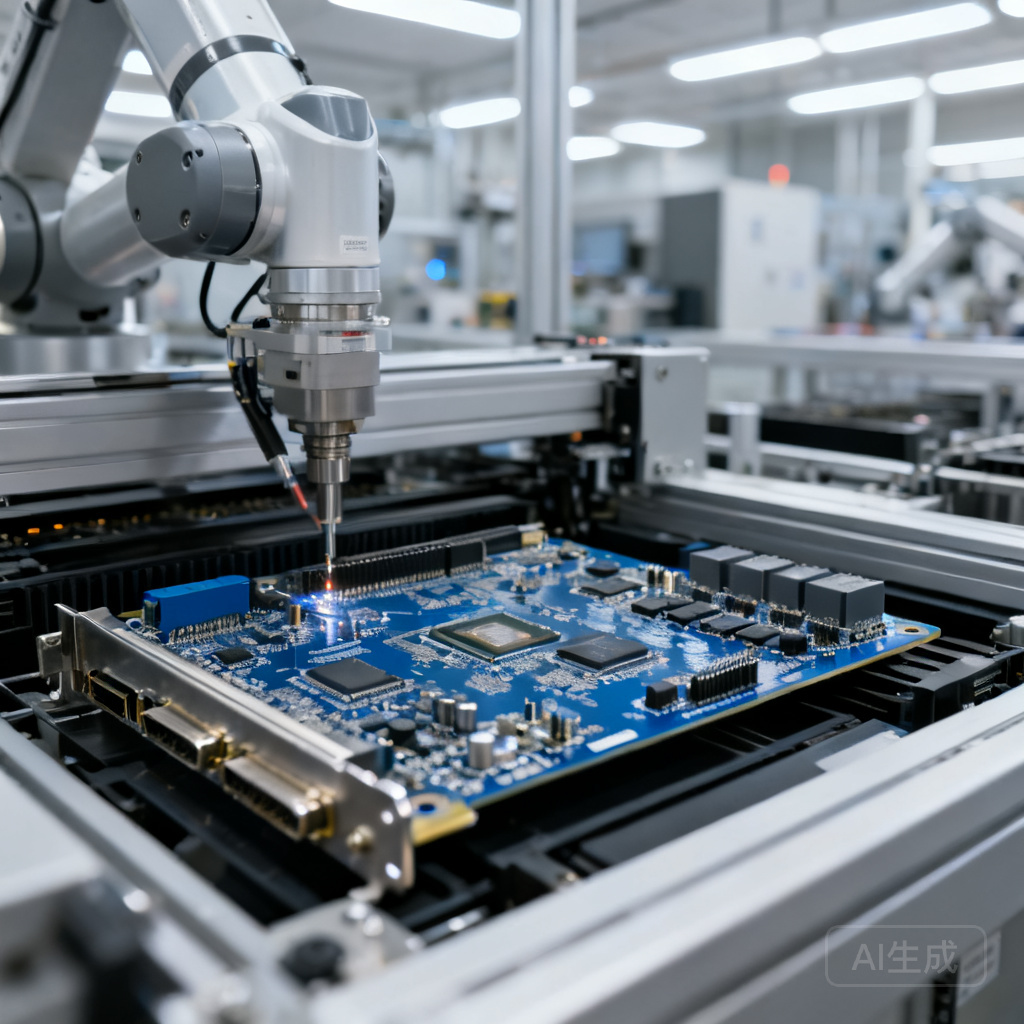
NovaPCBA specializes in high-performance PCIe Data Center Server Board Assembly, delivering precision manufacturing for cloud computing and AI workloads. Our advanced SMT lines and rigorous testing ensure signal integrity, thermal management, and reliability for Gen5/Gen4 PCIe interfaces. Trust our end-to-end turnkey solutions for scalable server infrastructure.
Overview
PCIe Data Center Server Board Assembly — NovaPCBA's Specialized Service
When a single PCIe Gen5 server board suffers via-in-pad voiding or glass-weave skew, the result isn't just a failed board—it's a rack-scale qualification stop and weeks of rework. Over 70% of electronic failures trace back to assembly quality issues, and 68% of BOMs contain messy data that triggers $250K rework cycles. NovaPCBA’s PCIe Data Center Server Board Assembly service eliminates these root causes through a fully integrated, ISO9001/IPC-A-610 Class 3 turnkey flow—from impedance-controlled stackup validation to 3D X-ray inspection of every BGA and press-fit connector. We serve hyperscale, AI/ML, and storage OEMs who need Gen4/Gen5 server boards assembled with zero-excursion reliability, not just “good enough” yields.
What's Included in Our PCIe Data Center Server Board Assembly
- SMT + THT Hybrid Assembly with Press-Fit Expertise: Fine-pitch SMT placement (0201, 0.4mm pitch BGA) alongside compliant-pin press-fit connectors for PCIe slots, DIMM sockets, and power connectors, all processed on a single line with in-line AOI after each reflow and wave stage.
- Impedance-Controlled PCB Fabrication & Signal Integrity Pre-Check: We validate stackup, trace geometry, and glass-weave alignment before assembly, referencing PCI-SIG board design guidelines to avoid the dielectric asymmetry that degrades Gen5 eye height on long CPU-to-slot paths.
- Full BGA & LGA Rework Capability: In-house BGA rework stations with profile-controlled IR/convection for large server-chip packages (e.g., Intel Xeon, AMD EPYC, retimers), preventing the latent open joints that often escape electrical test.
- Component Sourcing & Counterfeit Mitigation: Authorized distributor network with strict chain-of-custody; we reject the unqualified materials that cause 52% of product recalls.
- Functional Test & Margin Validation: PCIe link training, BER eye diagram testing, and full-speed loopback on representative server payloads—not just boundary scan—to catch intermittent failures that OEMs often miss until field deployment.
Assembly Approach Comparison
| Parameter | In-House Assembly (NovaPCBA) | Offshore-Only | Turnkey (NovaPCBA) |
|---|---|---|---|
| Lead Time | Prototype: 7–12 working days; volume: 3–4 weeks (domestic logistics) | Prototype: 4–6 weeks + customs; volume: 8–12 weeks with frequent delays | Prototype: 10–15 days (fab+assembly under one roof); volume: 4–5 weeks |
| Defect Catch | 3D AOI, X-ray, ICT at every stage; 100% BGA X-ray; real-time SPC | Often limited to post-reflow AOI; X-ray sampling only; no in-line process control | Full AOI, X-ray, flying probe/ICT, functional test—all in-house, no hand-offs |
| Cost Driver | Higher NRE but zero rework freight and no $50K+ per-change redesigns (85% of teams face up to $250K rework) | Low unit price, but hidden costs: rework shipments, line-down time, 46% of teams estimate $50K+ per change order | Competitive all-in cost with no supplier finger-pointing; cost of quality is built in, not discovered later |
| Failure Boundary | Single accountable partner; failure stops at our final QA gate, not your data center | Gaps between fab, assembly, and test; 52% of recalls stem from uncontrolled processes with no single responsible party | End-to-end ownership from laminate to loaded board; failure boundary is the shipped, tested assembly |
Industries & Applications
Hyperscale Data Center & Cloud Infrastructure: Multi-socket server motherboards, PCIe riser cards, and storage backplanes require Gen4/Gen5 signal integrity and high-current power delivery—assembled to IPC-A-610 Class 3 for 24/7 operation.
AI/ML Accelerator Platforms: Boards hosting 8× GPU or ASIC PCIe cards demand ultra-flat surface finishes, low voiding under large BGA packages, and precise press-fit alignment for high-speed connectors, all of which we verify with in-line 3D X-ray.
Enterprise Storage & NVMe-oF Appliances: Dense PCIe lane routing and mixed-signal layouts (PCIe clocks, sideband signals) need controlled impedance and low skew; our process includes TDR verification before component placement.
Telecom Edge & 5G Infrastructure: Server boards deployed in NEBS environments rely on robust THT soldering and conformal coating options that we integrate without secondary outsourcing.
Our Manufacturing Process
- DFM & Stackup Review: We cross-check Gerber data against PCI-SIG specifications for trace impedance, via stub length, and glass-weave orientation, flagging any long parallel runs that could cause Gen5 skew.
- Stencil & Solder Paste Application: Laser-cut stencils with nano-coating for fine-pitch pads; 3D SPI (solder paste inspection) on 100% of boards to catch insufficient or bridged deposits before placement—eliminating the root cause of over 70% of assembly defects.
- SMT Placement & Reflow: High-speed mounters handle 0201 passives and large server-chip BGAs; 10-zone reflow ovens with nitrogen atmosphere for low voiding (<10% under BGAs) and precise soak profiles per component datasheets.
- Press-Fit & Selective Wave Soldering: Compliant-pin connectors are pressed with force-monitored equipment to avoid cracked barrels; through-hole components on mixed-technology boards are soldered via selective wave or robotic soldering, preserving SMT integrity.
- Inspection, Test & Validation: 3D AOI post-SMT, 2D/3D X-ray for BGA and press-fit barrels, in-circuit test (ICT), and functional test with PCIe loopback and margin analysis—all before the board leaves our floor.
Quality Assurance
We assemble every PCIe Data Center Server Board to IPC-A-610 Class 2 or Class 3 criteria, as specified, with full traceability. Our multi-stage inspection regime catches defects at the point of origin: 3D solder paste inspection prevents printing errors; post-placement AOI checks component presence and polarity; post-reflow 3D AOI identifies lifted leads, tombstones, and solder bridges; X-ray inspection verifies BGA voiding (<10% per joint) and press-fit pin integrity. Flying probe or bed-of-nails ICT confirms passive values and short/open nets, while functional test runs actual PCIe link training and data patterns. This layered approach directly addresses the reality that most electronic failures originate in assembly. All processes are governed by our ISO9001:2015 quality management system, and we maintain RoHS compliance with full material declarations.
Frequently Asked Questions
- Q: How can we audit your process for PCIe Data Center Server Board Assembly before placing an order?
- A: We welcome on-site or virtual audits. You’ll review our SMT lines, X-ray and AOI equipment, BGA rework stations, and our ISO9001/IPC-A-610 workmanship certifications. We’ll also walk you through a recent server board build, showing first-article inspection reports, SPI data, and X-ray images of press-fit connectors. This is standard practice for hyperscale OEMs and proves we can meet your quality requirements without surprises.
- Q: What traceability and chain-of-custody documentation do you provide for components and bare PCBs?
- A: Every reel, tray, and bare board carries a unique lot code that links to our ERP. You receive a full Certificate of Conformance (CoC) listing manufacturer part numbers, date codes, and RoHS compliance. For high-reliability server boards, we can also supply X-ray fluorescence (XRF) reports and solder paste chemistry certifications. This addresses the supplier gaps that contribute to 52% of product recalls—we maintain a single, auditable chain from laminate to finished assembly.
- Q: What is the typical lead time for PCIe Data Center Server Board Assembly?
- A: Prototype quantities (1–10 boards) typically ship in 7–12 working days after Gerber and BOM approval, assuming components are in stock. Production volumes of 50–500+ units run 3–4 weeks. Turnkey orders that include our managed PCB fabrication and component sourcing add about 3–5 days to the prototype window but eliminate the multi-week delays common with offshore-only models. We also offer expedited 5-day prototype service for time-critical bring-up.
Get a Quote for PCIe Data Center Server Board Assembly
Upload your Gerber files, BOM, and any PCIe compliance test plans for a free, no-obligation quote. Our engineering team will review stackup, component availability, and test requirements within 24 hours—so you can move from design to data center validation with a single accountable partner. Start your quote now.
References & Further Reading
- Common PCBA Defect Analysis and Prevention – 86PCB
- Quality and Compliance in End-to-End PCB & PCBA Manufacturing – Ring PCB
- The Hidden Cost of Redesigning PCBs Around Missing Components – AccurisTech
- 6 Common Causes of PCB Failure – Matric
- PCI-SIG Specifications
- PCIe Board Design Guidelines – PCI-SIG (via TI E2E)
- Datacenter Server PCB Design Guide – HilPCB
- Intel Server Board M50FCP2SBSTD Technical Product Specification – Colfax