Optical Transceiver PCB Assembly
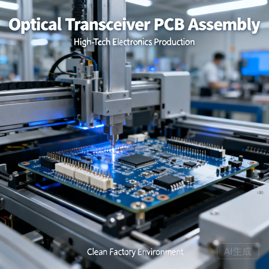
NovaPCBA delivers precision Optical Transceiver PCB Assembly for high-speed data communication networks. Our advanced SMT and micro-assembly processes ensure low signal loss, exceptional thermal management, and strict impedance control, enabling reliable performance in 100G, 400G, and beyond transceiver modules.
Overview
Optical Transceiver PCB Assembly — NovaPCBA's Specialized Service
When a single optical transceiver PCB assembly fails at 400G or 800G line rates, the result isn’t just a dead link—it’s unplanned downtime, costly truck rolls, and potential recall exposure. Common PCB failure modes like solder joint fatigue, via cracking, and contamination are magnified in high-density optoelectronic boards where TOSA/ROSA alignment tolerances are sub-micron. OEMs and network operators facing 52% of product recalls traced to unqualified raw materials or uncontrolled assembly need a manufacturing partner that treats every optical transceiver PCBA as a mission-critical component, not a commodity. NovaPCBA delivers IPC-A-610 Class 2/3 assembly with full process traceability, in-house AOI/X-ray, and a single-source accountability model that eliminates the blind handoffs responsible for most field failures.
What's Included in Our Optical Transceiver PCB Assembly
- SMT + THT hybrid assembly with in-line AOI: We place 0201 passives, fine-pitch BGAs, and press-fit cages on the same line, with automated optical inspection after every placement stage—catching misalignment, tombstoning, and solder bridging before reflow, as recommended by PCB reliability testing methodologies.
- Controlled impedance routing and thermal management: High-speed differential pairs for 25G/50G/100G lanes require strict impedance control (±10% or better). We use low-loss laminates and embedded copper coins to manage the heat from CDRs, drivers, and EMLs, directly addressing the thermal challenges outlined in the Juniper 800G optical transceiver guide.
- Active alignment and micro-optics integration: Our process includes precision die bonding and active alignment for TOSA/ROSA components, ensuring the optical sub-assembly meets the datasheet-specified link budget and interoperability targets.
- Full functional testing and burn-in: Beyond ICT and flying probe, we perform module-level functional tests (eye diagram, BER, optical power) and optional 24-hour burn-in to weed out infant mortality, a critical step given that testing and compliance documentation account for a significant portion of transceiver cost.
- Traceability and device history records (DHR): Every PCBA receives a unique serialized identifier linked to its full manufacturing record—components, operators, process parameters, and test results—creating the complete lineage that limits recall scope in the event of a field issue.
Comparison of Assembly Approaches
Choosing between in-house, offshore-only, or a turnkey partner has direct consequences on yield, lead time, and total cost of ownership. The table below draws on real-world trade-offs discussed in PCB manufacturing service comparisons and competitive PCBA benchmarks.
| Metric | In-House Assembly (NovaPCBA) | Offshore-Only | Turnkey (NovaPCBA) |
|---|---|---|---|
| Lead Time | 5–10 working days (prototype), 15–20 days (production) | 3–5 weeks plus shipping and customs | 7–15 working days (prototype), 20–25 days (production) with full supply chain visibility |
| Defect Catch | AOI, X-ray, and ICT at every stage; typical first-pass yield >98% | Varies widely; often limited to final visual inspection unless specified | Integrated inline AOI, X-ray, and functional test; defects caught before value is added downstream |
| Cost Driver | Higher NRE, but per-unit cost often lower than self-assembly once labor, depreciation, and yield losses are factored | Low labor rates, but hidden costs from rework, scrap, and logistics can erase savings | Optimized total cost: consolidated procurement, reduced rework, and no handoff delays |
| Failure Boundary | Single-source accountability; DHR traceability limits recall scope to exact affected batches | Fragmented responsibility; 52% of recalls stem from unqualified materials or uncontrolled processes with no single owner | End-to-end ownership from BOM to final test; full compliance documentation included |
Industries & Applications
Data Center Interconnects: 100G/400G/800G QSFP-DD and OSFP modules demand ultra-low bit error rates and strict thermal envelopes. Our assembly process supports the MSA form factors and IEEE standards that ensure multi-vendor interoperability.
Telecom & 5G Fronthaul: SFP28 and SFP56 transceivers for eCPRI links require extended temperature ranges (-40°C to +85°C) and high reliability. We use industrial-grade materials and processes validated for long-term outdoor deployment.
Medical & Industrial Laser Systems: Custom optical transceiver PCBA for laser drivers and photodetector circuits demand low noise, high voltage isolation, and biocompatible assembly. Our IPC-A-610 Class 3 capability meets these stringent requirements.
Automotive LiDAR & ADAS: Co-packaged optics and hybrid lidar transceivers need shock/vibration resistance and functional safety traceability. Our assembly aligns with IATF 16949-aligned process controls, including full component-level traceability.
Our Manufacturing Process
- DFM Review and Material Qualification: Our engineers cross-check your BOM against approved vendor lists, verify impedance stack-ups, and flag any components at risk of obsolescence. Only RoHS-compliant, traceable materials enter our facility, preventing the unqualified raw material issues cited in recall statistics.
- SMT Assembly and Reflow: High-precision pick-and-place machines handle 0201 passives and 0.4mm-pitch BGAs. Nitrogen reflow profiles are tuned for the specific thermal mass of optical transceiver boards, minimizing voiding and intermetallic growth.
- THT and Micro-Optics Integration: Through-hole cages, connectors, and heat sinks are wave or selective soldered. Active alignment stations position TOSA/ROSA components, referencing the internal structure described in optical transceiver component guides.
- Test and Validation: Flying probe or ICT verifies electrical integrity. Then, full functional test measures optical output power, extinction ratio, and receiver sensitivity against the datasheet specifications. Only boards passing all tests are serialized and packed.
Quality Assurance
Every optical transceiver PCBA undergoes a multi-stage inspection regime aligned with IPC-A-610 Class 2 or Class 3, as specified by the customer. Automated optical inspection (AOI) after solder paste printing, post-placement, and post-reflow catches solder bridges, insufficient solder, and misaligned components before they become latent defects. X-ray inspection verifies BGA and QFN solder joint integrity, identifying voiding and head-in-pillow defects that would otherwise escape electrical test. In-circuit testing (ICT) and flying probe confirm component values and net connectivity, while functional testing validates the assembly’s optical and electrical performance. Our ISO9001-certified quality management system ensures that every process is documented and auditable, and our device history records (DHR) provide the complete traceability needed to limit recall scope to precise batches. This multi-layered approach directly mitigates the common failure modes identified in PCB reliability analysis.
Frequently Asked Questions
- Q: How can I audit NovaPCBA’s process for optical transceiver assembly before placing an order?
- A: We welcome on-site and virtual audits. You’ll have access to our ISO9001 documentation, IPC-A-610 training records, equipment calibration logs, and sample DHRs. We can also run a first-article build with your BOM and provide full inspection reports, including AOI images and X-ray shots, before committing to production volumes.
- Q: What certificates of conformance (CoC) and traceability documentation do you provide with each shipment?
- A: Each shipment includes a CoC referencing the IPC-A-610 class, RoHS compliance, and the unique serial numbers of the assembled boards. We also supply a digital device history record (DHR) that links each serial number to its component lots, process parameters, and test results, enabling precise batch isolation if a field issue ever arises—exactly the kind of accountability missing in recall-prone supply chains.
- Q: What is the typical lead time for Optical Transceiver PCB Assembly?
- A: Prototype quantities (5–50 units) typically ship within 7–10 working days after BOM and Gerber approval, assuming all components are in stock. Production volumes (500–5,000 units) run 15–20 working days. Turnkey orders may add 3–5 days for component procurement. Expedited services are available for critical builds.
Get a Quote for Optical Transceiver PCB Assembly
Send your Gerber files, BOM, and test specifications to our engineering team for a free, no-obligation quote. We’ll respond within 24 hours with a DFM review, lead time estimate, and a clear breakdown of costs—so you can move from prototype to production with a partner that takes full responsibility for your optical transceiver PCBA quality.
References & Further Reading
- 6 Common Causes of PCB Failure: What OEMs Should Know
- Quality and Compliance in End-to-End PCB & PCBA Manufacturing Service in 2026 - Ring PCB
- Overview of PCB/PCBA Reliability Testing and Failure Analysis | Altium
- PCBA - PCB & MCPCB - EBest Technology
- How to Compare PCB Manufacturing Services for Your Board | Altium
- PCB Assembly vs Competitors: TOPFAST vs JLCPCB vs PCBWay
- Why Are Optical Transceivers Expensive? Cost, Testing & OEM Markup
- PCB vs PCBA: Key Differences and Which Your Project Needs
- The Internal Components and Structure of The Optical Transceiver
- Optical Transceiver Datasheet Guide: SFP Specs & PDF Downloads
- Guide to Optical Transceiver Standards - Pro Optix
- Juniper 800G Optical Transceivers and Cables Guide