Motor Drive Inverter PCB Assembly
Optimize your power systems with our high-performance Motor Drive Inverter PCB Assembly. Designed for precision motor control, our assemblies deliver efficient energy conversion, robust thermal management, and long-term reliability in demanding industrial applications. From EV traction to factory automation, trust our expert assembly for seamless integration.
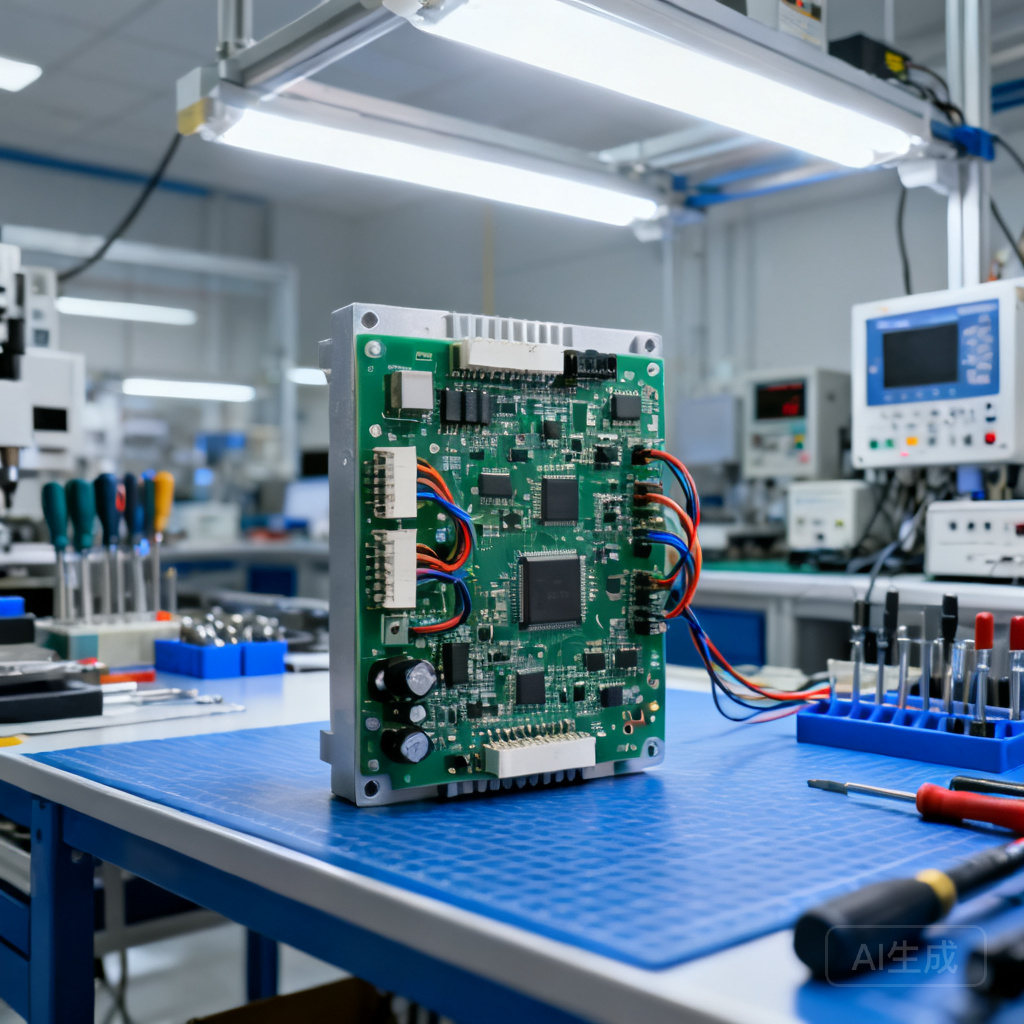
Overview
Motor Drive Inverter PCB Assembly — NovaPCBA's Specialized Service
When a single void in an IGBT solder joint can trigger shoot-through and field failure, procurement teams face a hard choice: trust assembly lines that treat power electronics like consumer PCBs, or partner with a specialist who understands that a motor drive inverter is a high‑current, high‑voltage, thermally stressed system. NovaPCBA’s Motor Drive Inverter PCB Assembly service eliminates that risk. We combine heavy‑copper SMT, selective THT for press‑fit pins and busbars, and multi‑stage AOI/X‑ray inspection to deliver boards that meet IPC‑A‑610 Class 2/3 — the standard expected in EV traction inverters and industrial drives where reliability directly impacts uptime and warranty cost.
What's Included in Our Motor Drive Inverter PCB Assembly
- Hybrid SMT + THT assembly with AOI at every stage: Surface‑mount gate drivers, current sensors, and passives are placed and reflowed, then through‑hole IGBTs, busbars, and large connectors are inserted and selectively wave‑soldered. Automated optical inspection after reflow and after wave soldering catches tombstoning, bridging, and insufficient fillets before they escape the line.
- Heavy copper capability (up to 10 oz): High‑current traces for phase outputs and DC‑link are formed on thick copper inner and outer layers, keeping current density low and temperature rise manageable — a critical requirement for motor control PCB thermal management.
- Impedance‑controlled routing for gate‑drive signals: Differential pairs for resolver and encoder feedback, and controlled‑impedance traces for high‑side/low‑side gate loops, follow layout practices that place bypass capacitors within 2 mm of driver ICs to minimise parasitic inductance, as recommended by Viasion.
- Thermal interface and substrate selection: We assemble on aluminium‑backed IMS (Insulated Metal Substrate) or FR‑4 with thermal vias, and apply phase‑change thermal interface material between power devices and heatsinks, ensuring junction temperatures stay within safe operating area during sustained full‑load testing.
- Functional test with motor emulator: Every assembled inverter board is run on a dynamometer‑style load that simulates a PMSM or induction motor, verifying gate‑drive timing, dead‑time insertion, current sensing, and fault protection before shipment.
Industries & Applications
Motor drive inverter PCBs sit at the heart of any system that converts DC to controlled AC. The assembly demands change with the application, but the failure boundary is always unforgiving.
- Electric Vehicle Traction Inverters: High power density (often >30 kW/L) and automotive vibration profiles require IATF 16949‑aligned process controls, 100% X‑ray of power‑device interconnects, and conformal coating to withstand coolant mist. Our assembly flow mirrors the discipline expected for automotive inverter PCB projects.
- Industrial Variable‑Frequency Drives (VFDs): Drives that run 24/7 in hot, dusty environments demand heavy‑copper PCBs with large creepage distances and robust press‑fit connectors. We validate solder joint integrity under thermal cycling from −40 °C to +125 °C, a regimen that exposes latent barrel cracks before they become field failures.
- Solar & Energy Storage Inverters: Bidirectional DC‑AC converters handling 1500 V DC buses need careful isolation management and partial‑discharge‑free assembly. Our selective conformal coating and controlled soldering profiles prevent dendrite growth that can lead to arc‑over in high‑humidity installations.
- HVAC Compressor Drives: Sealed compressor environments push PCB assemblies to survive refrigerant exposure and constant vibration. We use high‑Tg laminates and validated cleaning processes to avoid electrochemical migration, a common failure mode in these cost‑sensitive but reliability‑critical drives.
Assembly Strategy Comparison
Choosing the right sourcing model for motor drive inverter PCBs means balancing lead time, defect detection, and total cost of ownership. The table below contrasts three common approaches, drawing on real‑world service comparisons like TOPFAST’s analysis and insights from Hilelectronic’s cost‑benefit discussion.
| Factor | In‑House Assembly (NovaPCBA) | Offshore‑Only (Broker Model) | Turnkey (Single‑Source Partner) |
|---|---|---|---|
| Lead Time | 10–12 days prototype, 4–5 weeks production; all processes under one roof. | Often 6–8 weeks after factoring logistics and customs; delays when rework is needed. | Typically 3–5 weeks; supplier manages component sourcing and assembly, but visibility into sub‑tier quality varies. |
| Defect Catch | AOI after SMT and wave, X‑ray of power joints, ICT, and full functional test with motor load — defects caught before leaving the factory. | Relies on offshore partner’s inspection; often limited to AOI only, no functional test of the inverter stage. Defects discovered at system integration. | Depends on partner’s test investment. Many turnkey providers skip dynamic load testing for cost reasons; buyer must verify. |
| Cost Driver | Engineering‑intensive NPI and test development amortised over the product lifecycle; higher unit cost for very low volumes, but rework and field‑failure costs are minimised. | Low unit price, but hidden costs from rework, scrap, and engineering time spent debugging remotely. | Moderate unit price with procurement leverage; cost overruns occur when BOM changes or when functional test coverage is added late. |
| Failure Boundary | Process controlled to IPC‑A‑610 Class 3 for power sections; every board is powered up and stressed. Failures are contained to <0.1% at system integration. | High risk of latent defects (voids, cracked joints) that pass visual inspection but fail after thermal cycling. Failure discovered in the field. | Better than offshore‑only if partner has automotive‑grade lines, but still requires the buyer to audit test coverage. Automotive‑focused turnkey providers can achieve high reliability. |
Table informed by service comparisons from TOPFAST, Hilelectronic, and ChinaPCBA.
Our Manufacturing Process
- DFM Review & BOM Risk Assessment: We analyse the inverter schematic and layout for creepage/clearance violations, thermal relief on heavy copper, and component obsolescence. Feedback is delivered within 24 hours, often preventing re‑spins that delay NPI.
- SMT Assembly with 3D Solder Paste Inspection: After laser‑cut stencil printing (step‑up stencils for mixed‑component heights), 3D SPI verifies paste volume and shape before high‑speed placement of gate drivers, isolated DC‑DC modules, and passives. Reflow profiles are tuned for the board’s thermal mass, avoiding cold joints on large copper pours.
- Selective Wave Soldering & Press‑Fit: Through‑hole IGBT modules, DC‑link capacitors, and busbars are inserted and soldered using a selective wave system with nitrogen purge to minimise dross. Press‑fit pins for connectors and current sensors are seated with force‑monitored tooling, guaranteeing gas‑tight connections without thermal stress.
- Automated Optical Inspection & X‑Ray: AOI inspects every SMT and THT solder joint against IPC‑A‑610 Class 3 criteria (or Class 2 as agreed). For hidden joints under large power devices, 2D X‑ray checks void percentage in thermal pads and verifies solder ball integrity in BGAs, catching defects that optical systems miss.
- In‑Circuit Test & Full‑Load Functional Validation: ICT verifies component values, polarity, and shorts. The board then runs on a motor‑emulator test stand that applies rated DC‑bus voltage, drives a simulated motor load, and monitors phase currents, gate‑drive waveforms, and fault‑protection response. Only boards passing this dynamic test are shipped.
Quality Assurance
NovaPCBA’s quality system is built around ISO9001 and IPC‑A‑610, with RoHS compliance on all materials. For motor drive inverter assemblies, we default to IPC‑A‑610 Class 2 for general areas and Class 3 for high‑current, high‑voltage power sections — because a solder joint that looks acceptable under a microscope can still fail when it carries 100 A. AOI catches visible defects (bridging, insufficient solder, tombstoning) immediately after reflow and wave soldering. X‑ray inspection quantifies voiding in thermal pads and BGA balls, flagging anything above 25% void area — a threshold that directly impacts thermal impedance and long‑term reliability. In‑circuit testing verifies every resistor, capacitor, and diode against the BOM, while the functional test station runs the inverter at full rated power, confirming gate‑drive timing, dead‑time, and over‑current protection trip points. This multi‑layer defence prevents the latent failures that surface only after weeks of thermal cycling in the field. The layout discipline we enforce — such as placing bypass capacitors close to gate‑driver VCC pins, as detailed in Viasion’s design guide — is verified during DFM and re‑checked on first‑article boards, closing the loop between design intent and manufacturing reality.
Frequently Asked Questions
- Q: What should I audit when qualifying a supplier for Motor Drive Inverter PCB Assembly?
- A: Look beyond general SMT capability. Ask to see a process control plan for heavy copper (≥4 oz) and evidence of selective wave soldering for large THT components. Verify that the supplier can perform functional testing with a motor load — not just ICT. Request first‑article inspection reports per IPC‑A‑610 Class 3 for power sections, and confirm that X‑ray void analysis is part of the standard quality gate. A supplier who cannot show you how they manage thermal profiling for thick boards or how they validate press‑fit pin insertion force is unlikely to catch the defects that kill inverter drives.
- Q: How do you ensure traceability and provide a Certificate of Conformance (CoC)?
- A: Every assembly lot is assigned a unique serial number that ties to the component date codes, solder paste batch, reflow profile, AOI images, X‑ray records, ICT results, and functional test log. We maintain this data for a minimum of five years. The CoC we issue references the IPC‑A‑610 class accepted, the RoHS compliance status, and the test results, giving your incoming inspection team a complete chain of evidence.
- Q: What is the typical lead time for Motor Drive Inverter PCB Assembly?
- A: For prototype builds (5–20 boards) with all components in stock or available on short lead, we deliver in 10–12 working days, including DFM and functional test development. Production quantities of 500+ units typically ship in 4–5 weeks, depending on copper weight and BOM complexity. Expedited service can reduce prototype lead time to 7 days when component availability permits. We always provide a realistic schedule after BOM review, not before.
Get a Quote for Motor Drive Inverter PCB Assembly
Send your Gerber files, BOM, and any test specifications to our engineering team. We’ll return a detailed DFM report and a firm quotation within one business day — including lead time, test coverage, and any recommendations to improve yield. NovaPCBA’s commitment to IPC‑A‑610 quality means your inverter boards will perform from first power‑up to end of life.
References & Further Reading
- Inverter PCB: Types, Benefits, Selection Specifications, and More – OurPCB
- PCB Assembly vs Competitors: TOPFAST vs JLCPCB vs PCBWay – TOPFAST
- Inverter PCB: Cost, Benefits, and Applications – Hilelectronic
- Inverter PCB Assembly | Assembly PCB Inverter Manufacturer – ChinaPCBA
- Motor Control PCB: Design Guide for BLDC, AC and DC Motor Drives – HilPCB
- 2026 Top Inverter PCB Assembly for EVs What Buyers Need to Know – RichPCBA
- A Comprehensive Guide to Inverter PCB Design and Layout – Viasion