Marine Navigation PCB Assembly Solutions
Ensure precise marine navigation with NovaPCBA's Marine Navigation PCB Assembly Solutions. Our ISO9001/IPC-A-610 certified solutions tackle harsh maritime conditions, providing reliable performance for your vessels' critical systems. Discover how our expertise can elevate your marine navigation capabilities.
Overview
Marine Navigation PCB Assembly Solutions — NovaPCBA's Specialized Service
Our Marine Navigation PCB Assembly Solutions are designed for the marine industry, where reliability and precision are critical. Shipbuilders and marine equipment manufacturers need PCB assemblies that withstand saltwater corrosion and extreme conditions. NovaPCBA differentiates itself with over 15 years of experience, offering ISO9001 and IPC-A-610 standards compliance to ensure your marine navigation systems perform flawlessly.
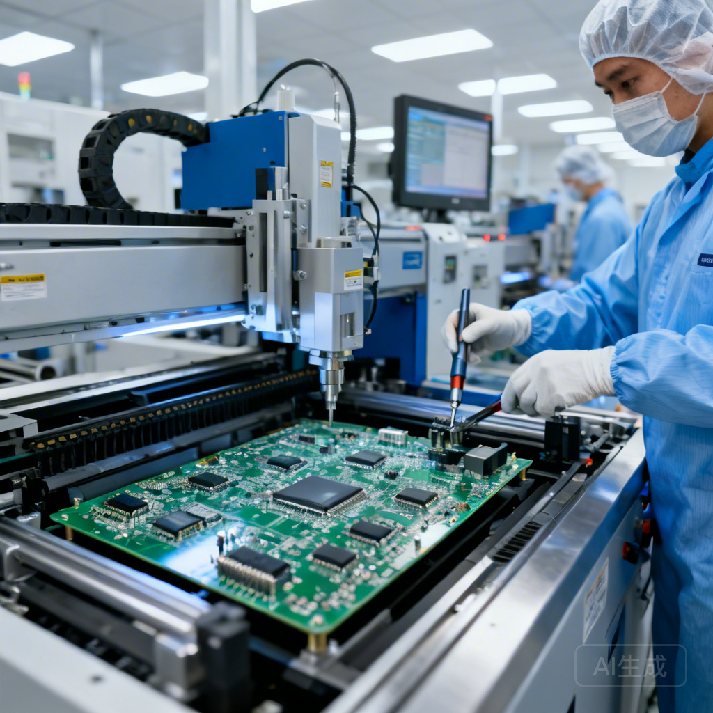
What's Included in Our Marine Navigation PCB Assembly Solutions
- Advanced Material Selection: Utilization of materials like FR-4 and specialized coatings for saltwater corrosion resistance.
- State-of-the-art Assembly Techniques: SMT + THT hybrid assembly with Automated Optical Inspection (AOI) at every stage.
- Comprehensive Testing: Includes In-Circuit Testing (ICT) and functional testing to ensure optimal performance.
- Custom Design Support: Engineering support for custom PCB layouts and designs to fit specific marine applications.
- Environmental Protection: IP69K-rated solutions for extreme environmental conditions.
Industries & Applications
Our solutions are integral to marine navigation systems, offshore communication setups, and underwater robotics. Each application demands robust PCB assemblies that resist environmental challenges. For example, offshore communication systems require reliable connections in harsh sea environments, while underwater robotics need durable, compact solutions.
Our Manufacturing Process
- Design Consultation: Initial assessment and consultation to understand specific needs and design requirements.
- Prototype Development: Rapid prototyping to test and refine designs before full-scale production.
- Assembly: Precision assembly using advanced equipment for SMT and THT techniques.
- Testing and Quality Control: Comprehensive testing processes ensure all assemblies meet stringent quality standards.
Quality Assurance
NovaPCBA’s quality assurance process includes compliance with IPC-A-610 Class 2 and 3 standards. Our assemblies undergo AOI to catch visual defects, X-ray inspection for hidden solder joint issues, ICT for circuit functionality, and functional testing to simulate real-world conditions. We are ISO9001 certified, ensuring consistent quality management.
Frequently Asked Questions
- Q: How does NovaPCBA ensure the durability of PCB assemblies in marine environments?
- A: We use corrosion-resistant materials and protective coatings to ensure long-lasting performance in harsh marine conditions.
- Q: Can NovaPCBA handle custom design requests?
- A: Yes, we offer custom design support to tailor PCB assemblies to your specific marine application needs.
- Q: What is the typical lead time for Marine Navigation PCB Assembly Solutions?
- A: Prototype development usually takes 2-4 weeks, while full production can range from 6-8 weeks depending on complexity and volume.
Get a Quote for Marine Navigation PCB Assembly Solutions
Contact us today to submit your Gerber files and BOM for a free quote. With our fast turnaround times, expert engineering support, and unwavering commitment to quality, NovaPCBA is your trusted partner for marine navigation PCB assembly solutions.