Machine Vision Camera PCB Assembly
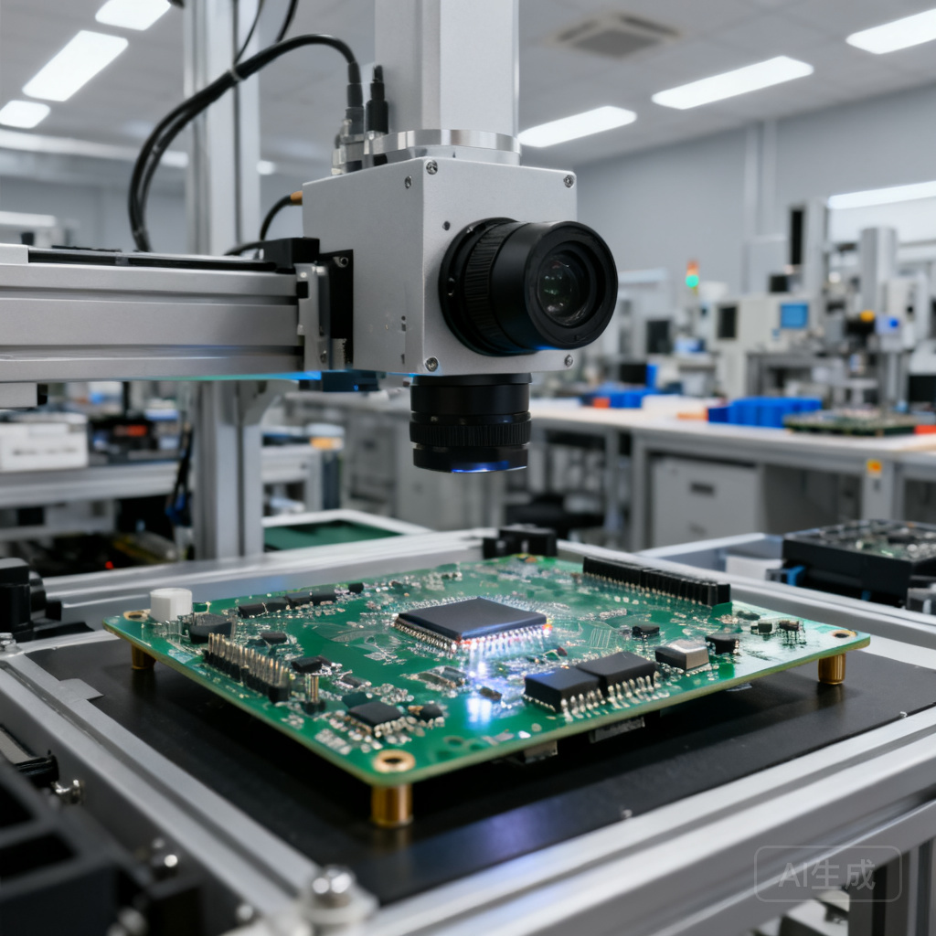
NovaPCBA delivers precision Machine Vision Camera PCB Assembly, integrating high-speed image sensors, low-noise analog front ends, and robust power management onto compact, high-layer-count boards. Our advanced SMT and micro-BGA processes ensure pixel-perfect signal integrity for industrial inspection, AI vision, and autonomous systems.
Overview
Machine Vision Camera PCB Assembly — NovaPCBA's Specialized Service
For engineering teams building industrial vision systems, smart cameras, or automated inspection equipment, a single component shortage in sensors, connectors, or FPCs can stall an entire production batch. A shortage or quality issue in sensors, ICs, connectors, FPCs, lenses, or power components can delay production or affect performance. When that happens, yield loss and rework costs escalate quickly. NovaPCBA’s Machine Vision Camera PCB Assembly service addresses this head-on with a fully managed supply chain, IPC-A-610 Class 3–aligned processes, and in-line AOI that catches placement errors before they become field failures. We combine deep experience in high-speed imaging boards with rigorous DFM feedback, so your camera modules deliver the signal integrity and thermal stability that inspection algorithms demand.
What's Included in Our Machine Vision Camera PCB Assembly
- SMT + THT hybrid assembly with multi-stage AOI: Fine-pitch SMT placement (down to 0201/01005) for image sensors and processors, plus through-hole connectors for rugged interfaces. Automated optical inspection runs after solder paste, post-placement, and post-reflow, referencing defect classification methods from morphological segmentation and image subtraction techniques that categorize 13 PCBA defect types into actionable groups.
- Controlled impedance and EMC-aware layout support: Our engineers review stack-ups for differential pairs (MIPI, USB 3.0, LVDS) and advise on trace geometry to maintain 100 Ω / 90 Ω impedance, critical for clean image data transmission. Design rules follow camera PCB EMC and thermal management principles to suppress noise in sensitive analog front-ends.
- Thermal management for high-resolution sensors: We integrate thermal vias, copper coin, or metal-core substrates to dissipate heat from image sensors and ISP chips, preventing dark current drift that degrades low-light performance. This is especially important for industrial camera PCB assembly operating in continuous capture mode.
- Component sourcing with shortage mitigation: Active BOM scrubbing against real-time distributor inventories avoids the sensor and connector bottlenecks highlighted by camera module PCB assembly supplier guides. We offer alternative parts with pin-to-pin compatibility and validate them through functional testing before production.
- ISP tuning and sensor-lens matching support: For customers requiring turnkey camera modules, we coordinate with optical partners to align lens CRA with sensor microlens arrays and provide initial ISP tuning parameters—reducing the iteration cycles that often delay projects, as noted in industrial vision camera module OEM guides.
Industries & Applications
Machine Vision Camera PCB Assembly serves applications where image fidelity directly controls a decision—inspection, measurement, or guidance. Typical industries include:
- Automated optical inspection (AOI) systems: Cameras that scan PCBAs for missing components or solder defects rely on high-bandwidth, low-noise boards. We build these with the same inspection rigor they will later perform, referencing AI-powered machine vision inspection architectures that detect micro defects on high-density boards.
- Robotics and autonomous vehicles: Embedded vision modules for SLAM, object recognition, and obstacle avoidance demand compact, thermally stable PCBA. Our processes align with the ruggedness required for automotive and CCTV camera PCB designs.
- Medical and scientific imaging: High-dynamic-range sensors and cooled camera cores need ultra-clean assembly to avoid leakage currents. We apply IPC-A-610 Class 3 workmanship and post-assembly cleaning to meet low-outgassing requirements.
- Security and surveillance: Multi-sensor panoramic cameras and IR-illuminated boards benefit from our hybrid SMT/THT capability, which securely mounts heavy connectors and lens holders while maintaining fine-pitch image sensor alignment.
Our Manufacturing Process
- DFM and stack-up review: Our engineers analyze Gerber files for impedance discontinuities, thermal relief, and component placement conflicts, referencing design-for-manufacturing (DFM) principles that differentiate bare PCB from full PCBA requirements.
- Solder paste inspection (SPI): 3D SPI verifies paste volume and alignment on fine-pitch sensor pads before placement, preventing opens or bridges that are invisible post-reflow.
- High-precision SMT and selective THT: Pick-and-place machines handle 01005 passives and BGA/LGA image sensors, followed by selective wave soldering for through-hole connectors, ensuring no thermal shock to sensitive optical components.
- Multi-stage AOI and X-ray: Post-placement AOI catches missing or shifted components early; post-reflow AOI uses threshold segmentation and XOR logic operations to detect solder defects. X-ray inspects BGA hidden joints, while SBC-based machine vision systems validate connector coplanarity and pin alignment.
- Functional testing and ISP validation: Boards are powered up with actual image sensors, and test patterns are captured to verify MIPI signal integrity, frame rate, and pixel defects. This step mirrors the connector and signal verification needs critical for reliable power and data transfer.
Quality Assurance
Every Machine Vision Camera PCB Assembly is built to IPC-A-610 Class 2 or Class 3 standards, with acceptance criteria verified at each stage. Our AOI systems use morphological algorithms and image subtraction techniques—validated by research from Ibrahim, Indera Putera, and Kaur et al. (comprehensive review of surface defect detection on PCBs)—to classify defects into actionable categories. For high-density boards, we deploy AI-based inspection models that have demonstrated 99%+ recall in detecting missing components and micro defects (AI vision inspection for manufacturing). X-ray inspection verifies BGA voiding below 25% per IPC-7095, and in-circuit testing (ICT) confirms passive values and short/open networks. Functional testing with the actual image sensor ensures that every board meets its specified frame rate and noise floor before shipment. Our facility is ISO9001-certified and RoHS-compliant, with full traceability from component lot codes to final assembly records.
Frequently Asked Questions
- Q: How do you audit and qualify your camera module PCB assembly suppliers?
- A: We maintain a single, ISO9001-certified manufacturing center where all processes are under our direct control. For specialized components like lenses or IR filters, we audit partner factories against IPC validation services criteria, reviewing process capability (Cpk) for critical dimensions and cleanliness. Every batch includes first-article inspection reports and cross-section analysis for via reliability. This integrated approach avoids the quality gaps common in distributed supply chains.
- Q: What certificates of conformance and traceability do you provide?
- A: Each shipment includes a Certificate of Conformance (CoC) referencing the IPC-A-610 class used, RoHS compliance, and a unique serial number linking to the full manufacturing lot history. Traceability extends to component date codes, solder paste lot, reflow profile, AOI defect images, and functional test logs. For Class 3 builds, we also provide X-ray images and cross-section micrographs upon request.
- Q: What is the typical lead time for Machine Vision Camera PCB Assembly?
- A: Prototype quantities (5–20 units) with all components in stock can be assembled in 7–10 business days, including DFM review and functional testing. Production volumes of 500+ units typically ship in 3–4 weeks, though expedited options are available at a premium (standard lead times are typically a few weeks, but expedited options come at a premium). Lead time ultimately depends on component availability; our BOM scrubbing and alternative sourcing can compress delays caused by allocation, as highlighted in camera module PCB assembly supplier guides.
Get a Quote for Machine Vision Camera PCB Assembly
Send your Gerber files, BOM, and any test specifications to our engineering team for a free design-for-manufacturability review and same-day quotation. We’ll identify potential impedance or thermal risks before you commit, and our sourcing experts will flag long-lead components immediately. With NovaPCBA, you get fast turnaround, transparent quality data, and a partner who understands the signal integrity demands of imaging systems.
References & Further Reading
- Camera Module PCB Assembly Supplier Guide – HCDPCBA
- AI-Based PCB Inspection with Machine Vision and Robotic Imaging – Intelgic
- AI Vision Inspection for Manufacturing: Automated Defect Detection Guide 2026 – iFactory
- A comprehensive review of research on surface defect detection of PCBs based on machine vision – ScienceDirect
- Industrial Vision Camera Module OEM Guide – HCDPCBA
- PCB Manufacturing & Assembly Inspection – Cognex
- PCB vs PCBA: Key Differences and Which Your Project Needs – Sierra Assembly
- Guide to Camera PCB: Components, Applications & 6 Design Rules – ELEPCB
- PCB Camera Assembly for Industrial and Consumer Applications – PCBONLINE
- Development of SBC based machine-vision system for PCB board assembly Automatic Optical Inspection – IEEE Xplore