Laser Engraver Control Board Assembly
Optimize your laser engraving machine with a professional Laser Engraver Control Board Assembly from NovaPCBA. We deliver high-precision PCB fabrication and component sourcing, ensuring stable motion control, reliable laser firing, and seamless connectivity for intricate engraving projects.
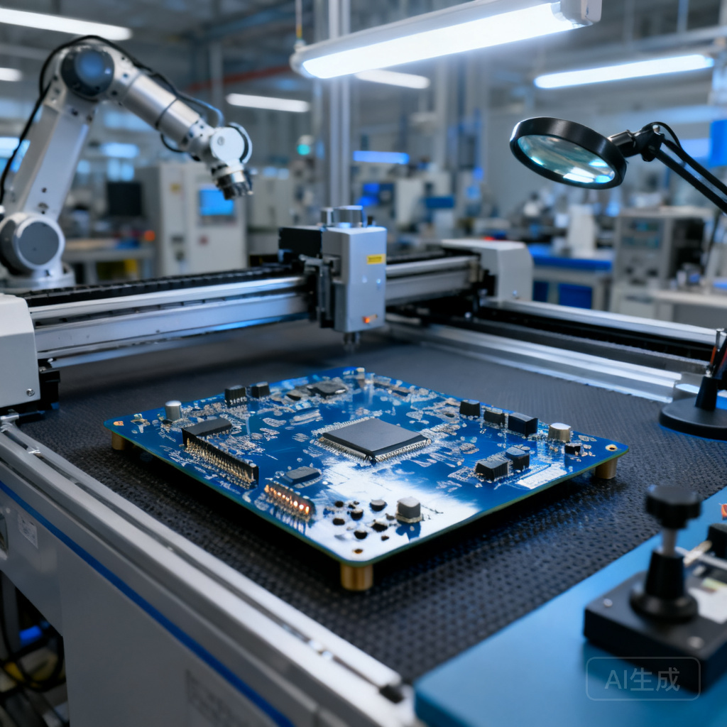
Overview
Laser Engraver Control Board Assembly — NovaPCBA's Specialized Service
When a laser engraver control board fails mid-job, the result isn't just a ruined workpiece — it's lost production time, thermal runaway risk, and warranty exposure. We've seen boards where poor solder joints on high-current laser driver stages caused intermittent PWM delivery, producing visible banding artifacts on engraved surfaces. NovaPCBA's Laser Engraver Control Board Assembly service addresses these failure modes at the process level: controlled impedance routing for step/direction signal integrity, selective solder paste deposition on power MOSFET pads, and 100% AOI on mixed-signal sections where analog laser feedback loops meet digital control logic. We build to IPC-A-610 Class 2 as standard, Class 3 by specification — because a control board that drifts under thermal load isn't just a nuisance, it's a precision defect generator. As industry comparisons between laser engraving and professional PCB fabrication highlight, the gap between hobbyist-level etching and production-grade assembly directly determines engraving repeatability and edge definition.
What's Included in Our Laser Engraver Control Board Assembly
- SMT + THT Hybrid Assembly: Laser control boards typically combine fine-pitch SMT components (MCUs, DACs, op-amps for analog feedback) with through-hole power devices (MOSFET drivers, terminal blocks, large electrolytic capacitors). We run dual-process lines — SMT reflow first, then selective wave soldering for THT — preventing thermal shock to sensitive SMT parts. Every stage includes AOI inspection per standard PCBA manufacturing process guidelines.
- Controlled Impedance & Signal Integrity: Step and direction traces between the MCU and stepper drivers must maintain consistent impedance to prevent pulse skew. We verify impedance on 4-layer and 6-layer stackups using TDR measurement, ensuring clean edge transitions that prevent missed microsteps — a common root cause of positional drift in engraving patterns.
- Thermal Management Assembly: Laser driver stages dissipate significant heat. We apply thermal vias under power ICs, specify copper weight (2oz minimum on power planes), and ensure proper heatsink mounting for TO-220 packages. Poor thermal assembly here leads to MOSFET Rds(on) drift, which alters laser tube current and produces inconsistent engraving depth across a job.
- Full BOM Sourcing & Counterfeit Mitigation: We procure all components — from STM32-series MCUs to Trinamic stepper drivers and optocouplers — through authorized distributors with full chain-of-custody documentation. For long-lead-time parts, we offer pin-compatible alternatives with engineering approval, as referenced in turnkey PCBA service models that emphasize cost-effective BOM management without compromising traceability.
- Laser Marking & Reference Designator Clarity: Every board receives crisp laser-marked reference designators (R1, C5, U3), polarity indicators, and pin-1 markings — essential for field servicing and manual rework. As noted in technical guides on laser engraving PCB boards, clear markings serve as the assembly and repair "map" for technicians, and we treat this as a non-negotiable quality output.
Industries & Applications
Laser engraver control boards serve a range of applications where precision motion control intersects with regulated laser power delivery. Desktop and industrial CO₂ laser engravers require boards that synchronize X/Y stepper pulses with PWM laser modulation — timing jitter here translates directly to visible artifacts on acrylic, wood, and coated metals. Fiber laser marking systems demand faster pulse trains and tighter current regulation for metal ablation; these boards often incorporate galvanometer control loops where signal integrity on differential pairs is critical. Medical device marking stations (UDI compliance, surgical instrument traceability) require control boards built to IPC-A-610 Class 3 with full traceability — a single marking failure can trigger a lot-level nonconformance. PCB prototyping engravers that use diode lasers for resist ablation, similar to the DIY diode laser etching approaches, need control boards with precise low-current analog feedback to prevent substrate damage during raster scanning.
Our Manufacturing Process
- DFM Review & Stackup Validation: We review Gerber files for manufacturability — checking annular rings, solder mask clearances, and thermal relief on power planes. For laser control boards, we pay particular attention to isolation between high-current laser driver sections and low-noise analog feedback traces, recommending stackup changes when crosstalk risk is identified.
- Solder Paste Application & SMT Placement: Using laser-cut stainless steel stencils (stepped thickness where needed for mixed-component designs), we apply solder paste with controlled aperture ratios. Fine-pitch QFP and QFN packages common on MCU-based control boards receive focused placement verification via SPI (Solder Paste Inspection) before reflow.
- Reflow & Selective Wave Soldering: SMT components undergo controlled-profile reflow with ramp-soak-spike parameters matched to the board's thermal mass. Through-hole connectors, terminal blocks, and large capacitors then pass through selective wave soldering — avoiding secondary reflow stress on already-placed SMT parts.
- AOI, ICT & Functional Testing: Automated optical inspection checks every solder joint against IPC-A-610 criteria. For production volumes, in-circuit testing verifies resistor networks, capacitor values, and diode orientation. Functional testing then validates the complete signal chain: stepper pulse outputs, PWM modulation linearity, and laser enable/disable logic — simulating real engraving sequences.
Quality Assurance
We build every Laser Engraver Control Board Assembly to IPC-A-610 Class 2 as our baseline, with Class 3 available for medical, aerospace, and high-reliability marking applications. Our QA framework is staged to catch defects at the point of origin: SPI after paste deposition catches insufficient or bridged deposits before components are placed; post-placement AOI verifies component presence, polarity, and tombstoning; post-reflow AOI inspects every visible solder joint for wetting, voiding, and fillet geometry per IPC-A-610 criteria. For BGA and QFN packages common on modern MCU-based control boards, X-ray inspection verifies void percentage and ball collapse. Functional test fixtures then validate the board under load — driving stepper outputs at maximum step rate while modulating the laser PWM channel, confirming that thermal rise doesn't induce timing drift. All processes operate under our ISO9001-certified quality management system, and every assembly is RoHS compliant. As Altium's guidance on comparing PCB manufacturing services emphasizes, the difference between services often lies not in advertised capabilities but in the rigor of inline inspection — and we apply inspection at every stage where a defect can be introduced.
Assembly Strategy Comparison
Choosing the right assembly model for laser engraver control boards directly impacts yield, lead time, and total cost of ownership. The table below compares three common approaches, informed by published PCBA service comparisons and our own production data:
| Metric | In-House Assembly (DIY Line) | Offshore-Only (Unmanaged) | Turnkey with NovaPCBA |
|---|---|---|---|
| Lead Time | Unpredictable — dependent on operator availability and rework cycles; typically 3–6 weeks for a batch of 50 units with debugging | 4–8 weeks including shipping and customs; delays from BOM shortages are communicated reactively, not proactively | 10–15 business days for prototypes; 3–4 weeks for production runs — with proactive BOM risk alerts before procurement begins |
| Defect Catch | Visual inspection only — cold joints, insufficient wetting, and tombstoning on fine-pitch components are routinely missed until functional test | Varies widely; many offshore providers run AOI but may not inspect 100% of joints on mixed-technology boards; X-ray is often an upcharge | SPI + pre-reflow AOI + post-reflow AOI + X-ray (BGA/QFN) + ICT + functional test — defects caught at the stage where rework cost is lowest |
| Cost Driver | Hidden: engineering time spent on rework, scrapped boards, and opportunity cost of diverted technical staff | Visible unit price is low, but cost of poor quality emerges later — field failures, warranty returns, and brand damage from inconsistent engraving performance | Transparent NRE + unit pricing; the primary cost lever is volume, not quality — we don't reduce inspection coverage to hit a price point |
| Failure Boundary | At the limits of operator skill — inconsistent soldering on power MOSFETs leads to thermal cycling failures that appear weeks after deployment | At the limits of communication — specification gaps (e.g., solder mask expansion on high-voltage traces) go unnoticed until creepage failures occur in humid environments | Defined by IPC-A-610 class and agreed acceptance criteria — failure boundary is explicit, inspected against, and documented in the Certificate of Conformance |
Sources: Assembly model distinctions drawn from TOPFAST PCBA competitor analysis and Altium's PCB manufacturing service comparison framework. Inspection stage data reflects NovaPCBA's documented process flow.
Frequently Asked Questions
- Q: Can we audit your facility before placing a production order for laser engraver control boards?
- A: Yes. We encourage supplier audits — particularly for customers whose laser control boards serve regulated industries. During an audit, you'll walk the SMT line, review our AOI and X-ray stations, inspect our ESD-controlled assembly floor, and examine our ISO9001 documentation. We can also provide first-article inspection reports and process capability data from previous laser control board builds. Contact our engineering team to schedule; we typically accommodate audits within two weeks of request.
- Q: What traceability documentation do you provide — do we get a Certificate of Conformance and component-level traceability?
- A: Every Laser Engraver Control Board Assembly ships with a Certificate of Conformance (CoC) referencing the work order, IPC-A-610 acceptance class, and RoHS compliance. For full traceability — required in medical device marking and aerospace applications — we provide lot-level traceability reports linking every component on the BOM to its manufacturer, date code, and distributor source. This extends to laser-marked board-level serialization when specified, enabling field-failure tracing back to the specific assembly batch. Our component procurement exclusively uses authorized distributors; we do not source from open markets where counterfeit risk is elevated.
- Q: What is the typical lead time for Laser Engraver Control Board Assembly — prototype versus production?
- A: Prototype quantities (5–25 units) typically ship in 10–15 business days from Gerber and BOM approval, assuming all components are in stock. Production runs (100–5,000+ units) run 3–4 weeks. The primary lead-time variable is component availability — we flag long-lead-time parts during the DFM review and offer pin-compatible alternatives before procurement begins, so you're never surprised by a delay after the order is placed. Rush service (7–10 business days for prototypes) is available with priority scheduling.
Get a Quote for Laser Engraver Control Board Assembly
Send your Gerber files, BOM, and any assembly notes to our engineering team for a same-day quote. We'll review your design for manufacturability, flag any potential issues with thermal relief or signal integrity on laser driver sections, and return a detailed quotation covering NRE, unit pricing, and lead time. Whether you're iterating on a prototype or scaling to production, our Laser Engraver Control Board Assembly service delivers the inspection rigor and process control that precision engraving applications demand.
References & Further Reading
- Laser Engraving vs. Professional PCB Fabrication — JLCPCB Blog
- How to Compare PCB Manufacturing Services for Your Board — Altium / CircuitMaker Pro
- PCB Assembly vs Competitors: TOPFAST vs JLCPCB vs PCBWay
- PCBA vs PCB: A Complete Guide to Printed Circuit Board Assembly Services — SFXPCB
- S27-1-1 Implementing Laser Marking of Printed Circuit Boards — Rick Stevenson, Electronics.org
- PCBA Manufacturing Process: Full-Step