Hearing Aid Miniature PCB Assembly
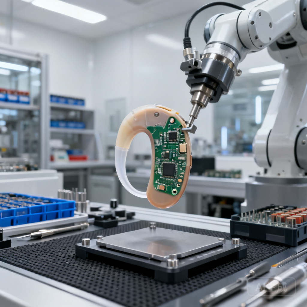
At NovaPCBA, we specialize in high-precision Hearing Aid Miniature PCB Assembly, delivering ultra-compact, reliable circuit boards for advanced hearing solutions. Our advanced SMT and micro-soldering processes ensure flawless performance in the smallest form factors, meeting strict medical device standards for clarity and durability.
Overview
Hearing Aid Miniature PCB Assembly — NovaPCBA's Specialized Service
When a hearing aid PCB fails at final test because of a cold joint on an 0201 capacitor—after six weeks of waiting for offshore boards—the real cost isn't the rework. It's the product launch delay, the FDA submission setback, and the engineering team pulled off their next project to troubleshoot what should have been caught at SPI. Over 40% of medical device companies experience product launch delays or recalls due to PCBA non-compliance or reliability defects. NovaPCBA's Hearing Aid Miniature PCB Assembly service exists to close that gap: ISO9001-certified, IPC-A-610 Class 2/3 qualified assembly with solder paste inspection (SPI) measuring volume, height, and area at every print cycle, plus AOI at every stage—so defects are caught before they leave the line, not after they reach your patient. We serve audiologists, medical device OEMs, and R&D teams who need miniature, high-density hearing aid circuit boards built right the first time, whether for behind-the-ear (BTE), in-the-canal (ITC), or completely-in-canal (CIC) form factors. Prototype and production runs are managed under one roof with full traceability—no broker handoffs, no blind offshoring.
What's Included in Our Hearing Aid Miniature PCB Assembly Service
- Micro-Miniature SMT Assembly (0201/01005): Full placement capability down to 01005 passives on flex and rigid-flex substrates—critical for CIC and IIC hearing aids where board real estate is under 8mm². Every placement is verified by post-placement AOI before reflow.
- Low-Temperature Solder Profiles for MEMS Microphones: Many hearing aid MEMS microphones have a maximum reflow tolerance of 240°C. We run SnBi or SnBiAg low-temp solder profiles with zone-by-zone thermal profiling to protect sensitive electroacoustic components during assembly.
- SPI + Pre-Reflow AOI + Post-Reflow AOI: Three inspection gates before a board leaves SMT. Solder paste inspection catches stencil wear and aperture clogging on 0.3mm-pitch pads. Pre-reflow AOI verifies component presence and polarity. Post-reflow AOI inspects every joint on every board—not just a sample batch.
- Conformal Coating for Moisture & Cerumen Resistance: Hearing aids operate in a high-humidity, acidic environment inside the ear canal. We apply parylene or acrylic conformal coating at controlled thickness (5–25µm) to protect against corrosion and cerumen ingress without adding bulk.
- Full Traceability & Lot-Level Documentation: Every component reel is scanned at feeder setup. Every board carries a unique serialized barcode linked to its full build record—paste lot, reflow profile, AOI images, and test results. Ready for FDA 21 CFR Part 820 and ISO 13485 audit trails.
Industries & Applications
Medical Hearing Aid OEMs: BTE, RIC, ITC, CIC, and IIC devices demand PCB assemblies that fit within shells as small as 6mm × 4mm. Our rigid-flex and multilayer HDI PCB assembly supports impedance-controlled traces for 2.4GHz Bluetooth LE and NFMI (near-field magnetic induction) links, with layer counts from 2 to 8 layers on polyimide or LCP substrates. Audiology Research & Clinical Trials: University labs and clinical researchers need 5–50 unit prototype runs with fast turnaround and engineering feedback on DFM issues. We review Gerber files for pad geometry, solder mask clearances, and via-in-pad risks before cutting a single stencil—catching design issues that cause tombstoning or insufficient solder on 0.4mm-pitch BGAs. Consumer Hearables & PSAPs: Personal sound amplification products and hearables require the same miniature assembly precision as medical hearing aids but at consumer price points. We optimize panelization and component sourcing to reduce per-unit cost without sacrificing AOI coverage or traceability.
Our Manufacturing Process
- DFM Review & Stencil Engineering: Every Gerber and BOM is reviewed by a process engineer. For hearing aid PCBs with 0.3mm-pitch CSPs or 0201 passives, we specify laser-cut stainless steel stencils with nano-coating, step-down thickness for fine-pitch zones, and aperture aspect ratios verified against the IPC-7525 standard.
- SPI & Solder Paste Application: Automated solder paste inspection measures volume, height, and area on every pad. Trending data flags stencil wear or squeegee pressure drift before it produces a single defect. This is the first containment gate—identifying material variability or alignment issues that cascade into reflow failures downstream.
- High-Speed SMT Placement with Vision Alignment: Components from 01005 passives to 0.4mm-pitch QFNs and MEMS microphone packages are placed on high-speed pick-and-place systems with fiducial correction at every placement cycle. For flex and rigid-flex boards, we use dedicated vacuum tooling plates to eliminate warpage during placement.
- Profiled Reflow & Post-Reflow AOI: Each board runs through a zone-controlled reflow oven with a profile tailored to the most thermally sensitive component on the BOM—typically the MEMS microphone or the DSP. Post-reflow AOI inspects 100% of solder joints for bridging, insufficient solder, tombstoning, and lifted leads, with defect images stored against the board's serial number.
Assembly Strategy Comparison
Engineering and procurement teams evaluating Hearing Aid Miniature PCB Assembly face a structural choice: build in-house, ship offshore, or work with a turnkey partner who manages the supply chain end-to-end. The table below compares the three approaches across the metrics that matter most for miniature medical PCB assembly—lead time predictability, defect containment, cost structure, and where failures are caught.
| Comparison Factor | In-House Assembly | Offshore-Only (Brokered) | Turnkey — NovaPCBA |
|---|---|---|---|
| Lead Time (Prototype) | 1–2 weeks (if capacity available) | 6–10 weeks (shipping + customs + rework loops) | 2–3 weeks (DFM-to-delivery, managed under one QMS) |
| Defect Catch Point | In-process (engineer on the line) | Post-shipment incoming QC—defects found weeks after build | Three-stage AOI (pre-reflow, post-reflow, pre-ship) with SPI trending at stencil level |
| Primary Cost Driver | Capital equipment amortization + skilled labor retention | Shipping, tariffs, and unbudgeted rework/re-spin costs | Managed NRE (stencil, fixturing, profile development) with transparent BOM costing |
| Failure Boundary | Caught internally during functional test | Found by end customer or regulatory audit—highest consequence | Caught at pre-shipment functional test gate; serialized traceability back to paste lot and reel ID |
Quality Assurance
Every Hearing Aid Miniature PCB Assembly we ship is built and inspected to IPC-A-610 Class 2 as standard, with Class 3 available for implantable-adjacent or life-critical hearing devices. Our QA architecture is built on four inspection gates, each catching defect classes that slip through the previous stage. SPI (Solder Paste Inspection): Measures paste volume, height, and area on every pad before placement—catches stencil aperture clogging, insufficient paste on 0.3mm-pitch pads, and bridging risks that AOI cannot see post-reflow because the defect is buried under the component body. Pre-Reflow AOI: Verifies component presence, polarity, and X-Y offset after placement but before reflow. This catches misplaced 0201 capacitors and rotated MEMS microphones—defects that become 10× more expensive to rework after reflow. Post-Reflow AOI: Inspects 100% of visible solder joints for IPC-A-610 Class 2/3 accept/reject criteria: bridging, insufficient solder, tombstoning, non-wetting, and lifted leads. Defect images are archived against the board's unique serial number for traceability. X-Ray Inspection (BGA/QFN): For boards with DSP BGAs or QFN packages with hidden thermal pads, we run 2D X-ray on 100% of production lots to verify void percentage (under 25% per IPC-7095) and pad coverage. Functional Test: Custom test fixtures validate audio path integrity, RF performance (Bluetooth LE pairing, NFMI link budget), and current consumption against the design specification. All test data is logged per serial number and included in the Certificate of Conformance. We are ISO9001:2015 certified and RoHS compliant. No fabricated quality metrics—just real inspection at every stage where defects are known to originate.
Frequently Asked Questions
- Q: How do we audit your assembly process before placing a production order for Hearing Aid Miniature PCB Assembly?
- A: We support both remote and on-site audits. For remote qualification, we provide a process capability package including first-article inspection reports, AOI defect rate trending across your prototype run, reflow profile data with thermocouple placement maps, and a full traceability sample linking one serialized board to its paste lot, component reels, and test results. For on-site audits, you can walk our SMT line, review our ISO9001:2015 quality manual, and inspect our ESD control program. We also accept customer-supplied audit checklists aligned to ISO 13485 or 21 CFR Part 820—many of our medical device customers use these as part of their supplier qualification process.
- Q: What traceability documentation do you provide—can we trace a field failure back to a specific component reel?
- A: Yes. Every board carries a unique serialized barcode. That serial number links to a build record containing: solder paste lot number and SPI data, component reel IDs and date codes for every part placed, the reflow profile time-temperature graph for that specific board, all AOI images (pre- and post-reflow), X-ray images if applicable, and functional test results. If a field return comes back, we can trace the failure to a specific reel, paste batch, or process deviation within 24 hours. This lot-level traceability is standard on every order—not an add-on.
- Q: What is the typical lead time for Hearing Aid Miniature PCB Assembly?
- A: For prototype quantities (5–50 units), typical lead time is 2–3 weeks from Gerber/BOM approval to shipment, assuming all components are in stock. Rush service at 7–10 business days is available with a surcharge. For production quantities (500–5,000 units), standard lead time is 4–5 weeks, including stencil fabrication, component procurement, SMT assembly, conformal coating, and functional test. Lead time is primarily driven by component availability—long-lead parts like DSP chips or custom-programmed EEPROMs can extend the schedule. We flag these during BOM review so you can make sourcing decisions before committing to a timeline.
Get a Quote for Hearing Aid Miniature PCB Assembly
Send your Gerber files, BOM, and target quantity to our engineering team for a same-day DFM review and quote. We'll flag any design risks—pad geometry, solder mask clearances, thermal relief—before you commit to a build. Fast turnaround, transparent pricing, and every board shipped with full traceability documentation. Submit your files here or email our team directly.
References & Further Reading
- PCB Assembly Trends OEMs Need to Know in 2026 | Foxtronics EMS — SPI and AOI inspection methodology, stencil wear detection, and material variability trending.
- Electronic OEM Prototype Hearing Aid PCB Printed Circuit Board Assembly SMD PCBA Service — China Dragon Electronic Industrial Co., Limited.
- Hearing Aid Circuit Board: How It Works & Key Features — Accio hearing aid PCB technical overview.
- Medical PCB Assembly: Reliability and Compliance Challenges — LSTPCB; cites 40%+ of medical device companies facing launch delays or recalls due to PCBA non-compliance.