EV Charging Controller PCB Assembly
Optimize your electric vehicle infrastructure with our advanced EV Charging Controller PCB Assembly. We deliver high-reliability, precision-manufactured boards that ensure seamless communication, power management, and safety compliance for Level 1 to DC fast chargers. Trust our expertise to accelerate your charging station production with zero-defect quality.
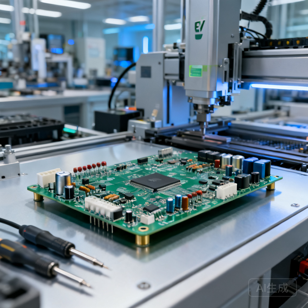
Overview
EV Charging Controller PCB Assembly — NovaPCBA’s Specialized Service
When a single power conversion system (PCS) failure can strand an entire fleet—as seen in recent Tesla Cybertruck PCS incidents—the cost of PCB assembly defects moves from a production metric to a brand crisis. NovaPCBA provides turnkey EV Charging Controller PCB Assembly engineered to eliminate the root causes of field failures: poor thermal management, uncontrolled impedance on high‑speed signal traces, and incomplete test coverage. We serve OEMs and EMS buyers who need IPC‑A‑610 Class 3 assemblies with full traceability, not just a low quote. Our process integrates in‑house DFM review, automated optical inspection (AOI) at every SMT stage, and functional testing under load, so your charging controllers meet the same reliability expectations as automotive‑grade electronics.
What’s Included in Our EV Charging Controller PCB Assembly
- SMT + THT Hybrid Assembly with Selective Wave Soldering: Mixed‑technology boards combining fine‑pitch surface‑mount components and high‑current through‑hole connectors are assembled on a single line, with selective soldering to avoid thermal shock to sensitive ICs. This is critical for power stages that carry 32 A and above.
- Controlled Impedance & High‑Voltage Isolation: We hold impedance tolerances to ±10% on differential pairs and maintain creepage/clearance distances per IEC 61851‑23 for 500 V+ circuits. Pre‑production impedance testing on coupons ensures signal integrity before assembly begins.
- Full Traceability from Raw Material to Shipment: Every PCB, component reel, and solder paste lot is barcoded and linked to the final assembly serial number. This end‑to‑end traceability—similar to the systems used by automotive PCB suppliers for recall management—enables rapid root cause analysis if a field issue ever arises.
- Multi‑Stage AOI & X‑Ray Inspection: Automated optical inspection after solder paste printing, post‑placement, and post‑reflow catches lifted leads, bridging, and tombstoning. X‑ray verifies BGA and QFN voiding below 25%, a threshold proven to reduce thermal fatigue in power modules.
- Functional Testing Under Real‑World Load Profiles: Assembled boards are tested with simulated AC/DC charging curves (e.g., CCS, CHAdeMO communication protocols) to validate voltage regulation, current sensing, and relay sequencing before leaving our facility.
Service Comparison: In‑House Assembly vs. Offshore‑Only vs. Turnkey
| Factor | In‑House Assembly (NovaPCBA) | Offshore‑Only Broker | Turnkey EMS Partner |
|---|---|---|---|
| Lead Time (prototype) | 5–8 working days with in‑house DFM and rapid prototyping; 3‑day expedite available for bare PCBs (similar to fast‑turn specialists) | 3–5 weeks due to shipping, customs, and language barriers | 10–15 days typical; longer if design files need translation |
| Defect Catch Rate | AOI at every stage + X‑ray + ICT; >99% first‑pass yield on Class 3 builds | Often limited to visual inspection; defects discovered only at final test | AOI and flying probe common, but process ownership fragmented |
| Cost Driver | Material & labor transparency; no hidden NRE; cost optimized through design feedback | Low unit price but high risk of rework, scrap, and air‑freight charges | NRE fees for test development; competitive on volume, less so on small batches |
| Failure Boundary | Failure contained to in‑house lot; traceability to component batch enables targeted recall | Failure can spread across multiple customer shipments; root cause often lost | Shared lines mean cross‑contamination risk; traceability depends on partner’s systems |
Comparison based on typical industry practices observed in EV charger PCB assembly services, EMS supplier selection guides, and vertically integrated factory models.
Industries & Applications
AC & DC Fast‑Charging Station Manufacturers: Wall‑box and public charging stations require controllers that manage power factor correction, ground fault detection, and OCPP communication. Our assemblies support the high‑voltage isolation and thermal cycling demands of 7 kW to 350 kW systems.
On‑Board Charger (OBC) Integrators: OBC modules must fit within tight automotive footprints while handling bidirectional power flow. We build dense, multilayer PCBs with embedded copper coins for heat dissipation, aligned with automotive EMS requirements for new energy vehicles.
Fleet & Depot Charging Infrastructure: High‑utilization chargers need redundant control boards that survive frequent plug cycles and wide temperature swings. Our conformal coating and underfill processes protect against moisture and vibration.
EVSE Communication Modules: Controllers handling ISO 15118 (Plug & Charge) require precise impedance control on high‑speed signal lines. We validate every board with time‑domain reflectometry (TDR) to ensure signal integrity for reliable vehicle‑to‑grid communication.
Our Manufacturing Process
- DFM & Design Review: We analyze Gerber files and BOM against IPC‑A‑610 Class 3 criteria, flagging potential issues like insufficient annular rings, acid traps, or component spacing that could lead to field failures. This step alone prevents the common mistake of underestimating testing requirements by building testability into the layout.
- Material Procurement & Verification: Components are sourced through franchised distributors with full lot traceability. For high‑voltage capacitors and relays, we perform incoming inspection including capacitance, ESR, and hipot testing to verify ratings before placement.
- SMT Assembly & Reflow: Solder paste is applied via laser‑cut stencils with step‑down thicknesses for fine‑pitch ICs. After pick‑and‑place, boards pass through a 10‑zone reflow oven with real‑time profiling to maintain a maximum slope of 2 °C/s, preventing thermal shock to ceramic capacitors.
- Through‑Hole & Selective Soldering: High‑current connectors and transformers are inserted and soldered with a selective wave system that applies flux only to the joints, eliminating the need for post‑solder cleaning and reducing contamination risk on sensitive analog front‑ends.
- Test & Validation: In‑circuit test (ICT) verifies component values and polarity; functional test simulates a full charging session, monitoring CAN/PLC communication, voltage ramp, and contactor timing. Final inspection under magnification confirms IPC‑A‑610 Class 3 workmanship.
Quality Assurance
Every EV Charging Controller PCB Assembly is built to IPC‑A‑610 Class 2 as standard, with Class 3 available for mission‑critical circuits. Our ISO9001‑certified facility uses a layered inspection strategy: AOI after solder paste print catches 100% of insufficient or bridged deposits; post‑placement AOI verifies component presence and polarity; post‑reflow AOI detects lifted leads, solder balls, and voiding anomalies. X‑ray inspection is mandatory for all BGA and QFN packages, with void percentage automatically calculated and flagged if exceeding 25%. ICT checks resistance, capacitance, and diode integrity, while functional test under load (up to 40 A AC) validates the controller’s response to over‑current, ground fault, and overtemperature conditions. All assemblies are RoHS compliant, and we provide certificates of conformance (CoC) with every shipment, linking the serial number to the complete manufacturing record—a practice that directly supports traceability requirements for automotive product recall management.
Frequently Asked Questions
- Q: How can I audit your manufacturing process before placing an order?
- A: We welcome on‑site audits and provide a detailed process capability study, including first‑article inspection reports, SPC data from recent EV charger builds, and our ISO9001 certification. Virtual audits via live video walk‑through are also available for international clients.
- Q: What documentation do you provide for traceability and compliance?
- A: Every shipment includes a Certificate of Conformance, a full material declaration (RoHS/REACH), and a unique serial‑number‑linked build record showing component date codes, solder paste lot, reflow profile, and test results. This package supports your own PPAP or regulatory submissions.
- Q: What is the typical lead time for EV Charging Controller PCB Assembly?
- A: Prototype quantities (5–20 boards) ship in 8–12 working days after Gerber/BOM approval. Production volumes (500+) typically deliver in 4–5 weeks. Expedited 3‑day bare PCB fabrication and 5‑day assembly are available for urgent development milestones, similar to fast‑turn EV charger PCBA services.
Get a Quote for EV Charging Controller PCB Assembly
Upload your Gerber files, BOM, and any test specifications to our secure portal for a free engineering review and same‑day quote. Our team will assess DFM risks, suggest cost‑saving alternatives, and confirm lead times—so you can move from prototype to production without surprises.
References & Further Reading
- Tesla Acknowledges Cybertruck PCS Failures – autoevolution
- EV Charger PCB: The Core of Safety and Reliability – HilPCB
- EV Charger PCB Solutions – POE
- Top 5 EV PCBA Mistakes Killing Your Production – JLCPCB
- EV Charger PCB Assembly Services – OurPCB
- EV Control System PCB Assembly: BMS, OBC & Charging Station Manufacturing – Venture Mfg
- High-Efficiency EV Charger PCBA with ISO/UL Certified Fast Lead Time – Ring PCB
- Cost-Effective EV Charger PCBA Manufacturing – Ring PCB
- Design Essentials for Smart EV Charging System Control – Ultra Librarian
- PCB Assembly for EV Chargers: An Essential Guide – Eashub