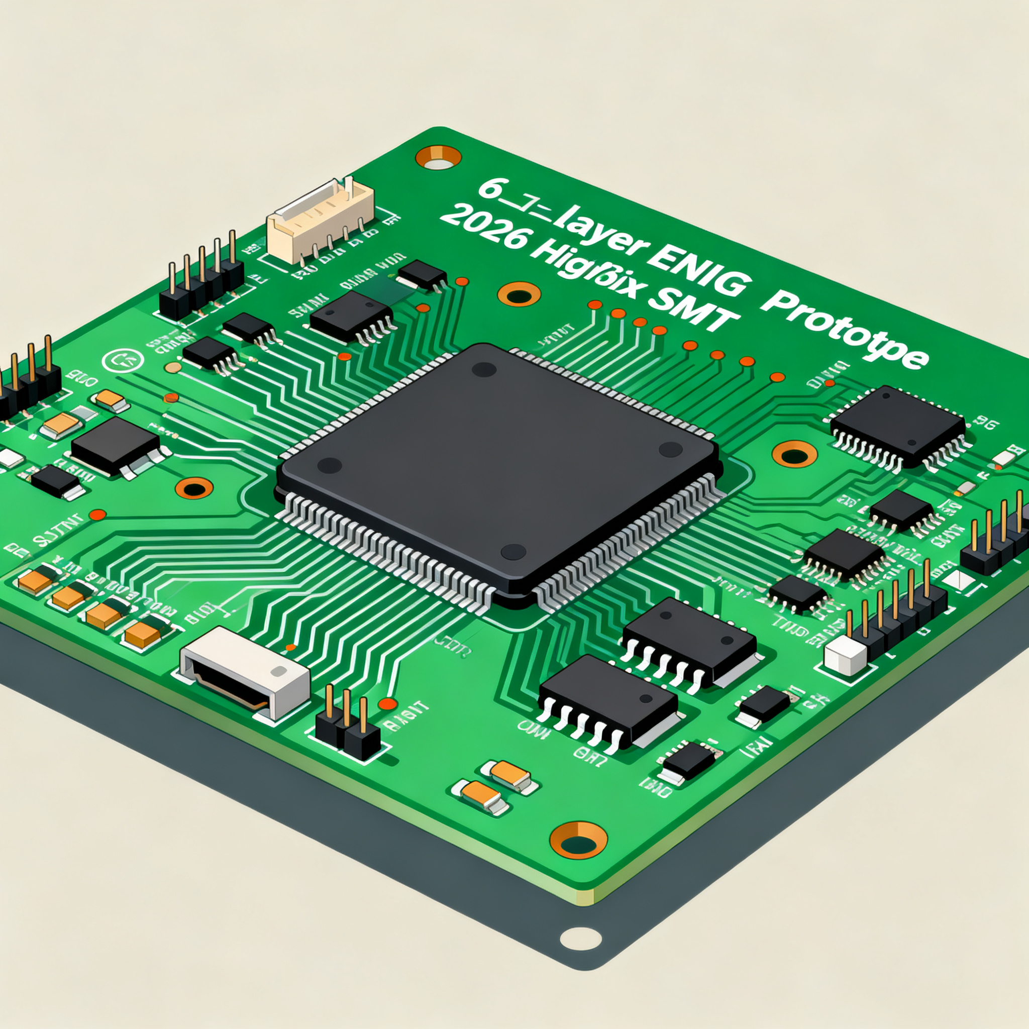
Wang PCB Assembly: 2026 High-Mix SMT Line Optimization for 6-Layer ENIG-Finished Prototype Runs
Why 6-Layer ENIG Prototypes Are Breaking Standard SMT Lines in 2026 You’ve seen the shift on your own desk: IoT sensor hubs, industrial edge controllers, and medtech wearables all demand 6-layer board...
Why 6-Layer ENIG Prototypes Are Breaking Standard SMT Lines in 2026
You’ve seen the shift on your own desk: IoT sensor hubs, industrial edge controllers, and medtech wearables all demand 6-layer boards with ENIG finishes for signal integrity, flatness, and wire-bonding readiness. The trouble is, most SMT lines were built for high-volume, low-mix manufacturing—4-layer HASL boards that run unchanged for weeks. When you throw a daily mix of 6‑layer ENIG prototypes at them, the line breaks down in ways that cost time, yield, and money.
JLCPCB’s recent analysis confirms that 6-layer PCBs are the sweet spot between cost and performance[1]. But the raw board cost alone illustrates the pressure: AllPCB’s data shows a jump from $0.50 per square inch for a 4‑layer build to $0.80 per square inch for a 6‑layer stack-up[2]. That’s a 60% premium before a single component is placed. When you couple that with ENIG’s sensitivity to reflow profile uniformity and the mixed-technology challenges of modern prototypes, a standard SMT line can quickly become a bottleneck.
The typical pain points: changeover times that stretch to 45–60 minutes between jobs, stencil alignment issues driven by ENIG’s flatness tolerance, and wave-soldering induced thermal shock on plated through‑holes that haven’t been sequenced properly. Engineers often see first-pass yields dip below 85% on initial 6‑layer ENIG runs, while procurement teams watch prototype lead times balloon to 10–15 business days. The root cause isn’t the board technology—it’s the assembly line’s inability to adapt to high-mix, low-volume demands.
Wang PCB Assembly recognized this gap early and set out to re‑engineer the SMT workflow from the ground up, specifically for 6‑layer ENIG prototype runs. The goal: a line that can switch between a complex RF board and a dense mixed-technology design in minutes, not hours, while keeping yields above 98%.
How Wang PCB Assembly Re-Engineered Its SMT Line for High-Mix Throughput
Wang’s optimization isn’t a single-machine upgrade—it’s a systemic rethinking of every step from kitting to final inspection. Four core principles drive the line: intelligent feeder management, modular setup carts, digital twin simulation for changeover, and inline SPI/AOI calibrated specifically for ENIG surface flatness. Each principle addresses a known failure mode in conventional high-mix assembly.
Intelligent feeder management replaces the traditional “one job, one feeder bank” model. Wang’s system uses smart feeders with RFID tags that automatically load the correct component reel, verify placement coordinates, and adjust pick-and-place parameters based on the specific 6‑layer board’s component density. This eliminates the manual setup errors that plague high-mix environments and cuts the feeder changeover time to under 10 minutes.
Modular setup carts allow operators to prepare the next job offline while the current job is running. A cart holds the stencil, solder paste, feeders, and any custom tooling for through-hole wave soldering. When the SMT line finishes a panel, the entire cart is swapped in a single motion, and the line’s digital twin instantly validates the new setup against the board’s CAD data. This is crucial for 6‑layer ENIG boards, where even a 0.05 mm misalignment can cause bridging on fine-pitch pads.
The digital twin simulation deserves special mention. Before a single physical board is loaded, the line’s software models the entire assembly sequence—screen printing, placement, reflow, and selective wave soldering—using the actual PCB stack-up and thermal properties. Analog Devices’ design note on multi‑layer thermal vias reminds us that heat must be dissipated to internal copper layers to prevent defects[3]. Wang’s digital twin incorporates these thermal paths, predicting reflow temperature gradients across the ENIG surface and adjusting the profile to maintain ±2°C uniformity. The result is a reflow recipe that works the first time, not after three iterations.
Inline Solder Paste Inspection (SPI) and Automated Optical Inspection (AOI) are tuned for ENIG’s reflective finish. Standard SPI systems often misread solder paste volume on bright gold pads, leading to false positives or missed defects. Wang’s calibrated lighting and algorithms differentiate between paste and pad reflections, achieving a 99.5% defect detection rate. AOI is similarly optimized for the fine-pitch components common on 6‑layer boards, referencing the exact pad geometry from the Gerber files.
PCBSync’s mixed-technology sequencing guide[4] emphasizes that SMT components should be placed and reflowed before through‑hole parts are inserted, and that wave soldering must be masked to protect sensitive SMDs. Wang’s line follows this sequencing but adds a dedicated pallet system for through‑hole connectors that shields the ENIG surface from direct solder wave contact, drastically reducing thermal shock and gold embrittlement risks.
The table below quantifies the difference between a standard SMT line and Wang’s optimized configuration for a typical 10‑piece, 6‑layer ENIG prototype run with 150 components (mixed SMT and through‑hole).
| Line Metric | Standard SMT Line | Wang Optimized Line | Impact on Prototype Delivery |
|---|---|---|---|
| Job changeover time | 45–60 min | 8–12 min | Enables 3–4 changeovers per shift instead of 1 |
| First-pass yield (ENIG, 6L) | 82–87% | 98.2% | Eliminates 2–3 rework cycles per board |
| Line utilization rate | 55–65% | 89% | Reduces idle time; more jobs per day |
| Stencil alignment accuracy | ±50 µm | ±15 µm | Critical for 0.4 mm pitch QFNs on ENIG |
| Wave solder thermal shock (ΔT) | Up to 180°C | ≤120°C (pallets) | Prevents via cracking and pad lifting |
These numbers are not theoretical. They come from Wang’s production logs for 6‑layer ENIG boards processed in 2025. The improvement in first-pass yield alone saves the typical prototype customer hundreds of dollars in rework labor and scrap, while the reduced changeover time means that a 10‑piece order can ship in 5–7 business days instead of 10–15.
Board design also feeds line performance. The Analog Devices thermal via guidelines[3] suggest placing thermal vias of 0.3–0.5 mm diameter under high-power components to dissipate heat into inner copper layers. When engineers follow this rule, the digital twin’s reflow simulation is more accurate, and the line can maintain its tight temperature control. Similarly, PCBSync’s[4] advice on sequencing mixed-technology boards—placing all SMDs first, then through‑hole connectors—aligns perfectly with Wang’s palletized wave process, reducing mask preparation time.
Wang’s Optimized Model vs. Traditional Contract Assembly: A 6-Layer ENIG Cost and Capability Comparison
How does Wang’s high-mix SMT line stack up against the alternatives you’re likely considering? The table below compares three distinct approaches: Wang’s optimized line, a low‑cost fab aggregator (represented by AllPCB and JLCPCB’s consolidated services), and a conventional high‑mix assembly shop that handles multiple technologies but hasn’t re‑engineered its changeover process. All data is normalized for a 6‑layer ENIG board, 100×80 mm, with a mixed BOM of 120 components.
| Comparison Metric | Wang Optimized Line | Low‑Cost Fab Aggregator (AllPCB/JLCPCB) | Conventional High‑Mix Shop | Selection Criteria & Failure Boundary |
|---|---|---|---|---|
| 6‑layer ENIG board cost (per sq in) | ~$0.80 (raw board) + assembly | $0.80 (AllPCB data[2]) | $0.80–0.90 (small‑batch premium) | Board cost is similar; the difference lies in assembly efficiency |
| Prototype lead time (10 pcs, mixed-tech) | 5–7 business days | 7–10 days (aggregated logistics) | 10–15 days | Choose Wang when time-to-test is critical; aggregators add shipping delays |
| Mixed-technology support (SMT + TH) | Full inline, palletized wave | Limited; often outsourced | Batch wave soldering | Wang’s pallet system protects ENIG; aggregators may reject complex TH |
| Design review depth | Free DFM check with stack‑up, thermal, stencil analysis | Automated rule check, no thermal feedback | Basic DFM, limited to manufacturing rules | Wang’s review references Analog Devices thermal rules[3]; aggregators miss thermally critical vias |
| Minimum order quantity | None (1 piece accepted) | Usually 5 pcs | Varies; often 10 pcs | Wang’s line is built for single‑piece NPI runs |
What the table doesn’t show is the cost of failure. JLCPCB’s 6‑layer analysis[1] underscores that the technology is mature, but the real value comes from how the board is assembled. A low‑cost aggregator can deliver a 6‑layer ENIG board for $0.80 per square inch, but if the assembly house doesn’t understand ENIG’s flatness requirements or the thermal demands of a mixed‑technology design, your first‑pass yield could drop to 80%. Reworking a 6‑layer ENIG board is expensive—each rework cycle risks lifted pads, solder mask damage, and voiding under BGAs. Wang’s line optimization eliminates these hidden costs.
Wonderful PCB’s stack‑up and cost‑reduction guidelines[5] recommend using standard lead times and working with the manufacturer’s design review to identify cost‑saving opportunities early. Wang’s free DFM check does exactly that: it flags potential issues like asymmetrical stack‑ups that could cause warpage, poor thermal via placement, and stencil aperture mismatches. The result is a board that arrives at the SMT line ready for high‑yield assembly, not a board that needs a quick design spin to fix field failures.
Designing 6-Layer ENIG Prototypes for High-Mix Assembly: 5 Rules That Save Time and Money
The best assembly line in the world can’t fix a poorly designed board. When you’re designing a 6‑layer ENIG prototype destined for a high‑mix SMT line, a few DFM rules can shave days off your lead time and dramatically improve first‑pass yield. These five rules distill the most critical advice from years of optimization at Wang and align with industry‑proven guidelines from Analog Devices, AllPCB, and PCBSync.
- Place thermal vias (0.3–0.5 mm) under every high‑power component. Analog Devices’ design note[3] states that multiple‑layer boards should use thermal vias under the thermal pad to dissipate heat to inner copper layers. AllPCB’s guide[2] specifies a diameter of 0.3–0.5 mm for these vias. Wang’s digital twin uses this information to model reflow profiles accurately. Skipping thermal vias leads to localized overheating, voiding, and ENIG discoloration.
- Keep the stack‑up symmetrical to avoid warpage during reflow. A 6‑layer board with an asymmetrical copper distribution will bow when heated, pulling fine‑pitch leads off the pads. Specify a symmetrical stack‑up (e.g., Signal‑GND‑Signal‑Signal‑GND‑Signal) and balance copper pour on outer layers. Wang’s DFM check flags asymmetrical designs automatically.
- Panelize for efficient stencil printing and handling. Individual 6‑layer boards are often too small for stable printing. Use a 2×2 or 3×2 panel with 5 mm rails and fiducials on each sub‑board. Wang’s setup carts are calibrated for these standard panel sizes, reducing changeover time further.
- Sequence mixed‑technology parts to minimize rework. Place all SMD components first, then through‑hole connectors. PCBSync’s comprehensive guide[4] warns that reversing the order forces manual soldering or re‑reflow, which degrades ENIG pads. Wang’s palletized wave process assumes this sequence, so sticking to it avoids special handling costs.
- Involve the assembler’s design review early—before you freeze the layout. Wonderful PCB’s experts[5] stress that working with the manufacturer’s design review identifies cost‑saving opportunities early. Wang’s free DFM check covers stack‑up verification, thermal via placement, and stencil aperture guidelines. A 15‑minute review can prevent a two‑week delay.
The table below summarizes the five rules, the key parameters to monitor, and the direct impact on assembly performance.
| DFM Rule | Key Parameter | Impact on High‑Mix Assembly | Reference |
|---|---|---|---|
| Thermal vias under hot components | Via diameter 0.3–0.5 mm | Reduces rework voids, improves reflow simulation accuracy | Analog Devices[3], AllPCB[2] |
| Symmetrical stack‑up | Cu balance ±10% per layer | Prevents warpage, maintains co‑planarity for fine pitch | Wang DFM rule |
| Panelization with fiducials | 5 mm rails, 2 fiducials per sub‑board | Speeds stencil alignment, reduces changeover time | Wang process requirement |
| SMD‑first sequencing | All SMDs reflowed before TH insertion | Eliminates manual rework, protects ENIG finish | PCBSync[4] |
| Early design review | DFM check before Gerber freeze | Cuts prototype lead time by 2–3 days, avoids respins | Wonderful PCB[5] |
These rules are not theoretical. In a recent case, a medtech customer brought a 6‑layer ENIG board with a power amplifier and dense QFN array. The initial design lacked thermal vias and had an asymmetrical inner layer. Wang’s DFM review caught both issues, and the revised layout passed the digital twin simulation with zero reflow anomalies. The result: 10 prototype boards delivered in 6 days, all passing functional test on the first pass.
Wang PCB Assembly High-Mix Optimization: What Engineers and Buyers Ask
Q: What turnaround time can I expect for a 10‑piece 6‑layer ENIG prototype with 100+ components?
A: Typically 5–7 business days. Wang’s accelerated kitting system stocks common passives, connectors, and ICs locally, and the digital setup—using the board’s CAD data to pre‑program feeders and reflow profiles—cuts the usual 2‑day preparation window to a few hours. Standard shops often quote 10–15 days for the same job because they batch similar orders and rely on manual changeover.
Q: How does Wang’s line handle mixed‑technology (SMT and through‑hole) on a 6‑layer board without compromising yield?
A: Wang uses a sequenced wave soldering approach after SMT reflow. All surface‑mount components are placed and reflowed first. Then, through‑hole connectors are inserted, and the board passes through a selective wave soldering machine equipped with dedicated pallets that shield the ENIG surface from direct solder wave contact. This method minimizes the thermal shock to the gold finish and prevents the pad lifting or intermetallic issues that plague conventional wave processes. The digital twin validates the entire thermal cycle before any physical board enters the line.
Q: Does using a 6‑layer ENIG stack‑up significantly increase assembly cost compared to 4‑layer HASL?
A: Yes, the raw board cost jumps from about $0.50 to $0.80 per square inch, as shown by AllPCB’s data[2]. However, the improved signal integrity and flat solderable surface often justify the premium—especially for prototypes where you need to validate performance, not just check connectivity. Wang’s line optimization reduces per‑unit assembly cost by eliminating rework and shortening setup time, which partially offsets the board cost increase. For a 10‑piece run, the total cost difference between 4‑layer HASL and 6‑layer ENIG might be only 15–20% higher, not 60%.
Q: What design reviews does Wang offer to catch DFM issues before prototype build?
A: Wang provides a free DFM check that covers stack‑up verification, thermal via placement, and stencil aperture guidelines. The review directly references the thermal management rules from Analog Devices[3] and AllPCB[2], ensuring that heat‑generating components have adequate vias to inner copper layers. It also checks for symmetrical stack‑ups, proper panelization, and mixed‑technology sequencing. The report comes back within 24 hours, often with screen‑annotated images of your Gerber files.
Q: Can I use standard 6‑layer stack‑ups from JLCPCB or Wonderful PCB and still get the benefits of Wang’s optimized line?
A: Absolutely. Wang’s line is compatible with most standard stack‑ups from JLCPCB[1] and Wonderful PCB[5]. However, Wang’s engineering team can suggest minor tweaks—such as adjusting the prepreg type or copper weight—to improve assembly yield on ENIG finishes. For example, if a standard stack‑up uses a resin‑rich prepreg that outgases during reflow, Wang’s DFM check will flag it and recommend an alternative that maintains the same impedance profile.
Q: What is the minimum order quantity for a high‑mix prototype run at Wang?
A: There is no minimum. Wang’s line is expressly designed for single‑piece or very low‑volume orders. The modular setup carts and digital twin simulation make it economically viable to run a single board without a setup charge penalty. This is ideal for engineering prototypes, proof‑of‑concept builds, and NPI runs where you may only need one or two functional units.
References & Further Reading
- Comparing 6-Layer PCBs with Other Multilayer PCBs: Cost, Complexity, and Optimization – JLCPCB
- Optimizing Mixed Technology PCB Assembly: A Guide to SMT and Through-Hole Integration – AllPCB
- SMT Assembly and PCB Design Guidelines for Leaded Packages – Analog Devices
- Mastering Mixed PCB Assembly: Complete Guide to SMT and Through-Hole Integration – PCBSync
- 6 Layers PCB Manufacturing: Advanced Stack-up, Design Guidelines, and Cost Analysis – Wonderful PCB
- SMT PCB Assembly: A Comprehensive Guide to Surface Mount Technology in Electronics – Wevolver
- Optimizing Mixed Technology PCB Assembly – AllPCB ElectroHub
For engineers and buyers who need a partner that understands the intricacies of high‑mix 6‑layer ENIG assembly, NovaPCBA offers similar SMT line optimization and design review services. Our PCB assembly capabilities are tuned for prototype and low‑volume orders, with a focus on quick-turn, high‑yield builds. Reach out to discuss your next 6‑layer ENIG prototype run and see how our process can cut your time‑to‑test.