Troubleshooting High Voltage Power Supply PCB Assembly: Common Pitfalls and Solutions
Troubleshooting High Voltage Power Supply PCB Assembly Introduction In the rapidly evolving world of electronics, the demand for high voltage power supply PCB assemblies is on the rise. These assembli...
Introduction
In the rapidly evolving world of electronics, the demand for high voltage power supply PCB assemblies is on the rise. These assemblies are critical components in various sectors, including industrial automation, medical devices, and telecommunications. Ensuring the reliability and efficiency of these assemblies is paramount, as any failure can lead to significant operational disruptions and financial losses. This article delves into the intricacies of troubleshooting high voltage power supply PCB assemblies, focusing on common pitfalls and providing actionable solutions. We will explore PCB layout rules, stackup design, signal integrity, and manufacturing considerations, equipping you with the knowledge to optimize your designs for performance and reliability.
Technical Overview
High voltage power supply PCBs are integral to converting and regulating electrical power in various applications. These PCBs must handle high voltages and currents while maintaining signal integrity and minimizing electromagnetic interference (EMI). The architecture of these boards typically involves multiple layers to accommodate complex routing and ensure adequate separation between high voltage and low voltage circuits. Key principles in designing these boards include maintaining appropriate trace widths and spacing, selecting the right materials for dielectric properties, and ensuring robust thermal management. Understanding these core concepts is crucial for designing PCBs that not only meet performance specifications but also adhere to industry standards such as those outlined by IPC.
Signal integrity is another critical aspect of high voltage PCB design. It involves managing the electrical performance of the PCB to prevent signal degradation, which can lead to data errors and component failure. This requires careful consideration of trace impedance, crosstalk, and return path integrity. Additionally, the choice of materials plays a significant role in the board's performance. Materials with appropriate dielectric constants and loss tangents must be selected to ensure the board can handle high frequency signals without excessive loss or distortion. By understanding these technical elements, engineers can design PCBs that are both efficient and reliable.
Detailed Specifications
When designing high voltage power supply PCBs, it's crucial to adhere to specific design rules and standards to ensure optimal performance and reliability. These specifications include trace widths, spacing, via sizes, and clearances, which are vital for managing electrical performance and preventing issues such as short circuits or signal interference. Understanding these specifications allows engineers to design PCBs that can handle high voltages while maintaining signal integrity.
| Design Rule | Specification | Importance |
|---|---|---|
| Trace Width | 0.25 mm (10 mils) | Ensures adequate current carrying capacity |
| Trace Spacing | 0.2 mm (8 mils) | Prevents arcing and short circuits |
| Via Sizes | 0.5 mm (20 mils) drill | Supports reliable interlayer connections |
| Clearance to Edge | 1.0 mm (40 mils) | Avoids edge-related shorts |
| Pad Sizes | 1.5 mm (60 mils) | Ensures proper soldering and mechanical stability |
| Solder Mask Clearance | 0.1 mm (4 mils) | Prevents solder bridging |
| Silkscreen Clearance | 0.15 mm (6 mils) | Avoids overlapping with pads |
| Minimum Hole Size | 0.3 mm (12 mils) | Facilitates component leads and vias |
| Impedance Control | ±10% | Maintains signal integrity |
| Aspect Ratio | 8:1 | Ensures manufacturability of vias |
Key Takeaways from the Specifications
The specifications outlined in Table 1 are critical for ensuring the reliability and performance of high voltage power supply PCBs. Proper trace width and spacing are essential to prevent overheating and electrical arcing, which can lead to catastrophic failures. The choice of via sizes and pad dimensions affects both the mechanical stability and electrical connectivity of the board. Ensuring adequate clearance to the edge and proper solder mask application are important to avoid shorts and solder bridging. Moreover, maintaining tight control over impedance is crucial for preserving signal integrity, especially in high-frequency applications. By adhering to these design rules, engineers can create robust PCBs that meet both functional and safety requirements.
| Layer Configuration | Description | Application |
|---|---|---|
| 2-Layer | Basic configuration with top and bottom layers | Simple designs, low cost |
| 4-Layer | Two signal layers, power, and ground planes | Improved EMI performance |
| 6-Layer | Four signal layers with dedicated power and ground planes | High-speed applications |
| 8-Layer | Six signal layers with power, ground, and shielding layers | Complex, high-density designs |
| 10-Layer | Eight signal layers plus power and ground | Advanced RF and microwave applications |
| 12-Layer | Ten signal layers with multiple power and ground layers | High-performance computing |
| 14-Layer | Twelve signal layers with additional power and ground layers | Data centers, telecom |
Practical Implications
The choice of layer stackup configuration significantly impacts the performance and manufacturability of high voltage PCB assemblies. A simple 2-layer stackup may suffice for basic designs with minimal complexity, offering a cost-effective solution. However, as the design complexity increases, additional layers become necessary to accommodate more signal routing and dedicated power and ground planes. This not only enhances EMI performance but also improves signal integrity and thermal management. For high-speed and high-density applications, opting for a 6-layer or 8-layer stackup allows for efficient routing and minimizes crosstalk. In advanced applications like RF and microwave, a 10-layer or more configuration is preferred to ensure optimal performance. Selecting the appropriate layer stackup is crucial for balancing performance requirements with cost constraints.
| Material | Dielectric Constant (Dk) | Loss Tangent (Df) |
|---|---|---|
| FR-4 | 4.5 | 0.020 |
| Rogers 4350B | 3.48 | 0.0037 |
| Rogers 4003C | 3.55 | 0.0027 |
| Nelco N4000-13 | 3.7 | 0.009 |
| Isola FR408HR | 3.68 | 0.009 |
| Arlon 85N | 3.5 | 0.004 |
| Megtron 6 | 3.2 | 0.002 |
| DuPont Pyralux | 3.4 | 0.003 |
| Taconic RF-35 | 3.5 | 0.0018 |
Application Guidelines
The selection of materials for high voltage PCB assemblies is guided by their dielectric properties, which influence the board's electrical performance. FR-4 remains a popular choice due to its affordability and satisfactory performance in many applications. However, for high-frequency applications where signal integrity is paramount, materials like Rogers 4350B and Megtron 6 offer lower dielectric constants and loss tangents, minimizing signal loss and distortion. For applications requiring exceptional thermal stability and low loss, materials such as Arlon 85N and Taconic RF-35 are preferred. Engineers must carefully evaluate the material properties in relation to the specific requirements of their application to ensure the PCB operates efficiently and reliably.
Design Considerations
Designing high voltage power supply PCBs involves several critical considerations to ensure optimal performance and reliability. First and foremost is the management of electrical and thermal loads. Adequate trace width and spacing must be maintained to handle the high currents and voltages without overheating or causing arcing. Thermal management is also crucial, requiring the use of heat sinks, thermal vias, or even active cooling solutions in high-power applications.
Signal integrity is another key consideration, particularly in high-speed applications. Careful routing of traces, maintaining consistent impedance, and minimizing crosstalk are all essential practices. The use of ground planes and careful layer stackup design can help mitigate EMI and ensure stable signal paths. Additionally, the choice of materials plays a significant role in the board's performance, with low-loss, high-frequency materials being preferred for RF and microwave applications.
Manufacturing considerations must also be taken into account during the design phase. This includes selecting the appropriate via sizes and aspect ratios to ensure manufacturability and reliability. Design for manufacturability (DFM) principles should be applied to facilitate efficient production and minimize defects. By considering these factors during the design phase, engineers can create PCB assemblies that are not only functional and reliable but also cost-effective to produce.
Step-by-Step Implementation
- Define Requirements: Begin by clearly defining the electrical and mechanical requirements of the high voltage power supply PCB, including voltage levels, current capacity, and environmental conditions.
- Schematic Design: Develop a detailed schematic diagram, ensuring that all components are correctly specified and that the circuit meets the required electrical parameters.
- PCB Layout: Perform the PCB layout, paying close attention to trace widths, spacing, and component placement. Use appropriate design rules to ensure thermal and electrical performance.
- Layer Stackup Design: Choose an appropriate layer stackup configuration based on the complexity of the design and the need for signal integrity and thermal management.
- Material Selection: Select materials with suitable dielectric properties to ensure the board can handle high frequencies and power levels without excessive loss.
- Simulation and Validation: Use simulation tools to validate the design, checking for signal integrity, thermal performance, and EMI compliance.
- Prototype Fabrication: Manufacture prototype boards using a reliable PCB fabrication service, ensuring adherence to industry standards and design specifications.
- Testing and Iteration: Test the prototype boards under real-world conditions, identifying any issues and making necessary design adjustments before mass production.
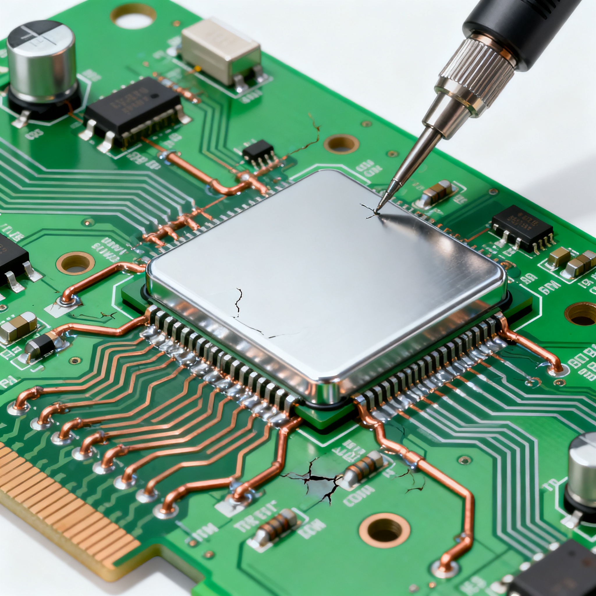
Common Issues & Solutions
- Overheating: Ensure adequate heat dissipation through the use of thermal vias, heat sinks, or active cooling solutions.
- Signal Integrity Problems: Maintain consistent trace impedance and use ground planes to minimize crosstalk and EMI.
- Solder Bridging: Apply accurate solder mask clearances and use appropriate pad sizes to prevent bridging during assembly.
- Component Misalignment: Use fiducials and proper alignment marks to ensure precise component placement during assembly.
- Insufficient Clearance: Ensure adequate spacing between traces and components to prevent arcing and shorts.
- Manufacturing Defects: Apply DFM principles and work with reputable PCB manufacturers to minimize defects and ensure quality production.
Applications & Use Cases
High voltage power supply PCBs are employed in a wide range of applications across various industries. In industrial automation, they are used to control and power machinery, ensuring efficient and reliable operation. In the medical field, these PCBs are integral to devices such as X-ray machines and MRI scanners, where precise power control is critical. The telecommunications industry relies on high voltage PCBs for signal transmission and power distribution in infrastructure such as cell towers and data centers. These applications highlight the importance of robust design and manufacturing practices to meet the demanding requirements of high voltage environments.
Selection & Sourcing Guide
Selecting the right components and materials for high voltage power supply PCBs is crucial for performance and reliability. Engineers should consider factors such as electrical specifications, thermal performance, and material properties when making selections. For sourcing components, IC Online offers a comprehensive range of electronic components, providing engineers with the resources needed to build and optimize their PCB designs.
FAQ
- What is the importance of trace width in high voltage PCBs? Trace width determines the current-carrying capacity of the PCB and is crucial for preventing overheating and ensuring reliable operation.
- How does layer stackup affect PCB performance? Layer stackup impacts signal integrity, thermal management, and EMI performance. More layers can accommodate complex designs and improve these aspects.
- Why is material selection important for high voltage PCBs? The dielectric properties of materials affect signal integrity and thermal performance, making careful selection essential for high-frequency and high-power applications.
- What are common causes of solder bridging? Solder bridging can occur due to inadequate solder mask clearance, incorrect pad sizes, or misalignment during assembly.
- How can I prevent signal integrity issues? Use consistent trace impedance, minimize crosstalk, and employ ground planes to maintain signal integrity.
- What role does thermal management play in PCB design? Effective thermal management prevents overheating, extends component life, and ensures reliable operation under high power conditions.
- How do I ensure manufacturability of my PCB design? Apply design for manufacturability (DFM) principles and work with experienced PCB manufacturers to optimize the design for production.
- What are the benefits of using advanced materials like Rogers or Megtron? These materials offer lower dielectric constants and loss tangents, making them ideal for high-frequency applications where signal integrity is critical.
- Can high voltage PCBs be used in consumer electronics? While high voltage PCBs are more common in industrial and medical applications, they can also be used in consumer electronics that require high power handling.
- What testing methods are used for high voltage PCBs? Common testing methods include electrical testing, thermal cycling, and EMI testing to ensure the board meets performance and reliability standards.
Conclusion
In conclusion, designing and troubleshooting high voltage power supply PCB assemblies require a comprehensive understanding of design rules, material properties, and manufacturing considerations. By adhering to industry standards and applying best practices, engineers can create robust and reliable PCBs that meet the demanding requirements of high voltage applications. The selection of appropriate materials, careful design of layer stackups, and attention to signal integrity and thermal management are all critical components of successful PCB design. By leveraging the insights and guidelines provided in this article, engineers can optimize their designs for performance, reliability, and cost-effectiveness.