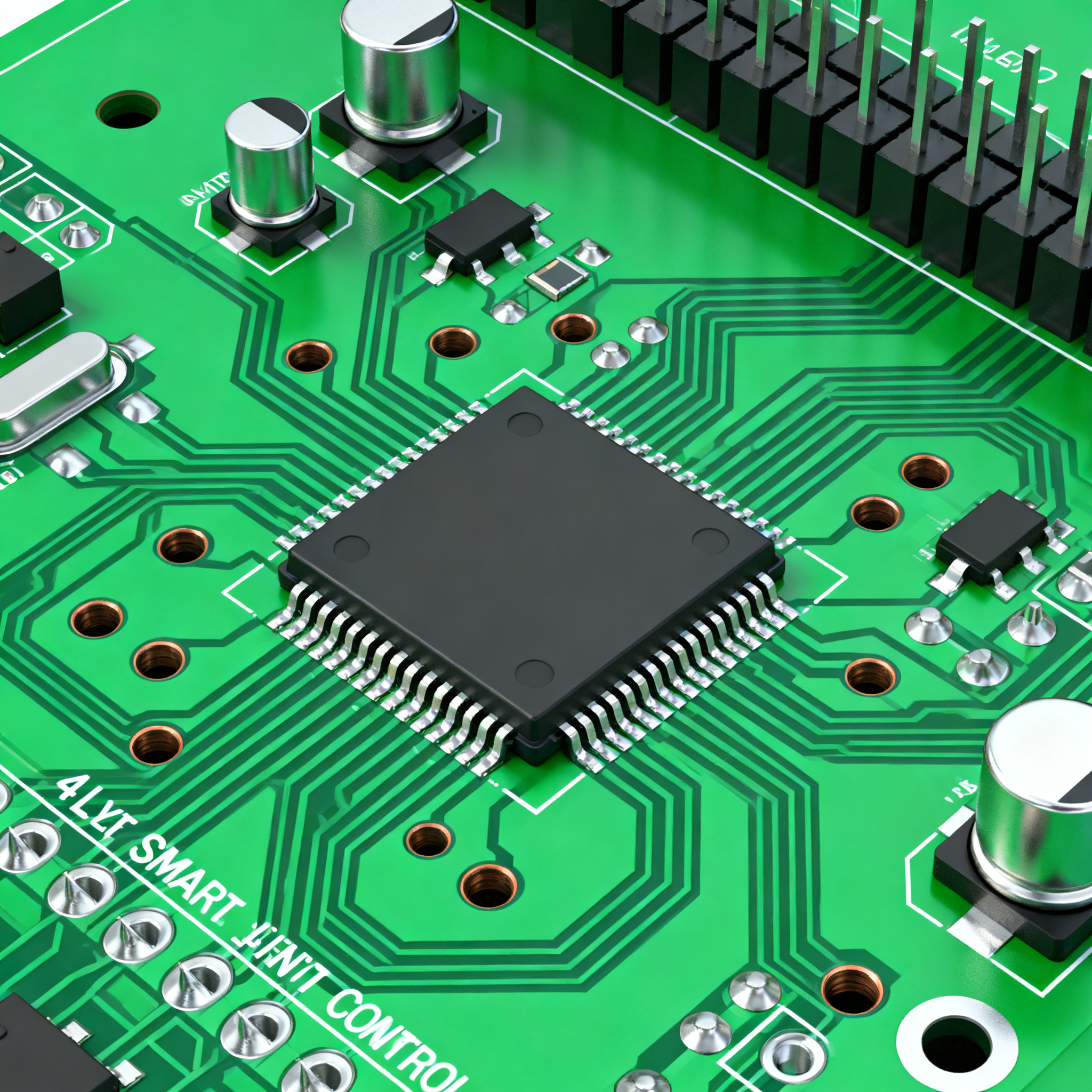
Troubleshooting EMI Failures in 4-Layer Smart Lighting Control PCBA Designs
Why 4-Layer Smart Lighting Boards Keep Failing EMI—and What’s at Stake Smart lighting control PCBAs sit at the intersection of wireless connectivity, high‑current LED driving, and aggressive cost targ...
Why 4-Layer Smart Lighting Boards Keep Failing EMI—and What’s at Stake
Smart lighting control PCBAs sit at the intersection of wireless connectivity, high‑current LED driving, and aggressive cost targets. A typical design packs a Wi‑Fi or BLE module, a microcontroller, one or more DC‑DC converters, and a multi‑channel PWM dimmer onto a 4‑layer board that must fit inside a compact luminaire or wall‑box. The result is a perfect storm for electromagnetic interference. When these boards go to the compliance lab, radiated and conducted emissions often exceed CISPR 15 or FCC Part 15 limits, triggering expensive redesigns and delaying product launches by weeks or months.
The pain is real. Tuya’s design requirements for lighting PCBA (Tuya) explicitly call out the need for controlled impedance, solid ground planes, and careful separation of power and digital sections—even on 4‑layer stacks. Yet many teams, pressed by BOM cost and board area, push these rules to the limit. EBest Technology’s experience with PCBA manufacturing (EBest) shows that test access and component selection often become afterthoughts, leaving EMI problems hidden until the first full‑system scan. The result: a board that works on the bench but fails in the chamber, or worse, causes flicker, resets, or Wi‑Fi dropouts in the field.
What’s at stake isn’t just a failed test report. A delayed certification can mean missing a retail season or a smart‑city tender. Field failures from EMI—such as a luminaire that randomly turns off because a BLE advertisement packet couples into the reset line—erode brand trust and drive up warranty costs. And in high‑volume production, every additional ferrite bead, shield can, or layout spin eats into margins that are already razor‑thin. Understanding why 4‑layer smart lighting boards keep failing EMI is the first step toward fixing them without blowing the budget.
How EMI Creeps into a 4‑Layer Lighting Control Stackup
Electromagnetic interference in a 4‑layer smart lighting PCBA rarely comes from a single source. It’s the cumulative effect of fast switching edges, poor return‑path design, and unintentional antennas formed by traces and copper pours. The frequency range of concern spans from a few kilohertz—where conducted emissions from switching regulators appear—up to several gigahertz, where harmonics of PWM dimming and wireless module clocks can radiate. Sierra Circuits’ EMI design guidelines (Sierra Circuits) note that most EMI problems occur between 9 kHz and 6 GHz, a band that covers virtually all the aggressors in a lighting control board.
In a typical 4‑layer stackup (signal‑GND‑PWR‑signal), the ground plane on layer 2 provides a return path for high‑speed signals on layer 1, but the power plane on layer 3 is often split or heavily perforated by vias and thermal reliefs. When a PWM signal transitions from low to high in a few nanoseconds, the return current must find a path back to the driver. If that path is interrupted by a gap in the reference plane, the current spreads out, creating a large loop area that radiates efficiently. The AllPCB EMC/EMI Q&A (AllPCB) emphasizes that reviewing ground routing and copper pours is the first step in any EMI investigation, precisely because discontinuous return paths are so common on cost‑optimized 4‑layer boards.
Switching noise from DC‑DC converters and LED drivers adds another layer of trouble. A buck converter switching at 500 kHz generates harmonics that can extend past 100 MHz. Those harmonics couple capacitively from the switch node to nearby traces, and inductively from the power inductor to any loop that shares flux. On a 4‑layer board without a dedicated shield layer, that noise easily finds its way onto the power rail that feeds the wireless module, degrading receiver sensitivity. The result is a Wi‑Fi module that works in isolation but loses packets when the LED channel is dimmed to 50%.
The table below summarizes the typical EMI frequency ranges and the aggressors most often responsible for failures in smart lighting control designs.
| Frequency Range | Typical Aggressor in Smart Lighting | Emission Type | Common Root Cause on 4‑Layer Boards |
|---|---|---|---|
| 9 kHz – 30 MHz | DC‑DC converter switching fundamental and low‑order harmonics | Conducted (power lines) | Insufficient input filtering; high‑impedance power plane |
| 30 MHz – 300 MHz | PWM dimming edges (LED driver outputs); buck converter switch‑node ringing | Radiated, conducted | Large current loops; missing stitching vias; poor ground referencing |
| 300 MHz – 1 GHz | Microcontroller clocks; high‑speed digital interfaces (SPI, I²C at fast mode); Wi‑Fi/BLE module harmonics | Radiated | Traces crossing split planes; antenna keep‑out violations; inadequate decoupling |
| 1 GHz – 6 GHz | Wi‑Fi/BLE fundamental and harmonics; DDR memory (if present); high‑speed USB | Radiated | Poor module grounding; lack of shielding; cavity resonances in enclosure |
Notice that the same physical mechanisms—discontinuous return paths, large loop areas, and unintentional coupling—appear across the entire spectrum. On a 4‑layer board, you have fewer degrees of freedom to fix them. The power plane is often a patchwork of polygons, and the bottom signal layer lacks a solid reference unless you pay careful attention to stitching. This is why many teams eventually ask whether a 6‑layer stackup is the only way out.
4‑Layer vs. 6‑Layer: When the Extra Cost Buys You a Cleaner Emissions Profile
The decision to move from 4 to 6 layers is never taken lightly in cost‑sensitive lighting products. A 6‑layer PCB typically adds 30–40% to the bare board cost, as detailed in Queenems’ 4‑layer vs. 6‑layer guide (Queenems). But that premium can be far cheaper than multiple EMC test cycles, delayed shipments, or field‑return campaigns. The key is knowing exactly what that extra pair of layers gives you in terms of EMI control.
A well‑designed 6‑layer stackup for smart lighting might be: signal‑GND‑signal‑PWR‑GND‑signal, or signal‑GND‑PWR‑GND‑signal‑signal. In both cases, you get two solid, uninterrupted reference planes that sandwich the high‑speed routing layers. This geometry slashes loop area because every signal trace has an adjacent return path. It also provides inherent shielding: the inner signal layer is buried between two planes, reducing radiated emissions. For designs with tight BGA fanout or multiple power rails that require low‑impedance distribution, the 6‑layer board becomes almost mandatory. Queenems notes that BGA pitch below 0.8 mm often forces a move to 6 layers just for routability, but the EMI benefit is a welcome side effect.
The table below compares the two stackup options across the metrics that matter most for smart lighting EMI performance.
| Comparison Metric | 4‑Layer Stackup (Signal‑GND‑PWR‑Signal) | 6‑Layer Stackup (Signal‑GND‑Signal‑PWR‑GND‑Signal) | Selection Criteria & Failure Boundary |
|---|---|---|---|
| Return path continuity | Good on top layer; poor on bottom layer unless stitched | Excellent on all signal layers; every trace has adjacent plane | If bottom‑layer emissions exceed limits despite stitching, 6‑layer is indicated |
| Power distribution impedance | Moderate; power plane often split, raising PDN impedance | Low; dedicated power and ground planes with close spacing | When voltage ripple on wireless module supply exceeds 50 mVpp, consider 6‑layer |
| Loop area for PWM and converter currents | Large; return currents must travel through vias and across splits | Small; tight coupling between power and ground planes | Radiated emissions above 200 MHz from LED driver loops often force a 6‑layer redesign |
| BGA fanout capability | Limited to 0.8 mm pitch and above with careful routing | Supports 0.5 mm pitch and multiple I/O rings | If the wireless module or MCU uses a fine‑pitch BGA, 6‑layer is the practical minimum |
| Cost adder (bare PCB, volume) | Baseline | +30% to +40% | Justified when one EMC retest costs more than the PCB premium across the production run |
For many smart lighting products, a 4‑layer board with disciplined layout can pass EMI. But when you’re fighting radiated emissions from a Wi‑Fi module that shares a board with a 2‑A LED driver, the physics starts to work against you. The 6‑layer stackup isn’t a luxury; it’s an insurance policy that often pays for itself in the first production batch by eliminating the need for hand‑soldered shielding cans and ferrite clamps.
Field‑Tested Fixes: Layout, Filtering, and Shielding for Smart Lighting PCBA
Before you commit to a 6‑layer respin, there’s a suite of 4‑layer‑friendly techniques that can bring a failing board into compliance. These fixes target the three main coupling mechanisms: conducted noise on power lines, radiated emissions from current loops, and direct module interference. Aivon’s practical EMI troubleshooting approach (Aivon) emphasizes near‑field scanning as the starting point—without knowing which component or trace is the dominant radiator, you’re just guessing.
1. Stitch the Ground Plane Aggressively. On a 4‑layer board, the bottom signal layer often lacks a continuous reference. Place ground vias (stitching vias) every 5–10 mm along the board perimeter and near any high‑speed signal transition. This creates a low‑impedance return path and suppresses edge radiation. Sierra Circuits’ 7 design tips (Sierra Circuits) highlight that stitching vias are essential whenever a signal changes reference planes, but on a 4‑layer board they also help contain fields within the PCB.
2. Separate Power and Digital Sections Physically. Keep the LED driver, its inductor, and the switching node on one side of the board, and the wireless module and microcontroller on the other. Use a solid ground plane as a barrier. Route noisy power traces away from sensitive analog and RF inputs. EBest Technology’s manufacturing insights (EBest) remind us that component placement for test access and thermal management often conflicts with EMI best practices; negotiate these trade‑offs early with your layout team.
3. Filter at the Source. A ferrite bead or small LC filter on the power input of the wireless module can knock down conducted noise by 10–20 dB in the 100–500 MHz range. Place the filter as close to the module pin as possible. For LED driver outputs, a series resistor‑capacitor snubber across the switching node damps ringing and reduces high‑frequency harmonics. The AllPCB Q&A (AllPCB) recommends ferrite cores on power leads as a quick diagnostic; if a clamp‑on ferrite on the DC input cable makes the emissions disappear, you know where to focus your filtering effort.
4. Shield the Wireless Module. If radiated harmonics from the module itself are the problem, a small snap‑on metal shield can over the module can provide 10–15 dB of suppression. Ensure the shield is well‑grounded to the board’s ground plane with multiple vias. This is often cheaper than a full 6‑layer redesign, especially for mid‑volume products.
5. Pre‑Compliance Scanning on a Budget. You don’t need a full anechoic chamber to find EMI hot spots. A spectrum analyzer with a set of near‑field probes (H‑field and E‑field) lets you scan the board and identify the exact inductor, trace, or IC that is radiating. For conducted emissions, a Line Impedance Stabilization Network (LISN) connected to the spectrum analyzer gives a reliable indication of pass/fail margins. Aivon’s guide (Aivon) walks through this process step by step, showing how to correlate near‑field scans with far‑field chamber results.
The table below summarizes common EMI fixes and their typical effectiveness in smart lighting designs.
| Fix | Typical Frequency Range Addressed | Approximate Improvement | Implementation Cost |
|---|---|---|---|
| Stitching vias along board edge | 30 MHz – 1 GHz | 3–8 dB reduction in radiated emissions | Zero (layout change only) |
| Ferrite bead on module VCC | 100 MHz – 500 MHz | 10–20 dB conducted noise reduction | $0.02–0.05 per bead |
| RC snubber on switching node | 50 MHz – 300 MHz | 6–12 dB reduction in ringing harmonics | $0.03–0.08 per snubber |
| Metal shield can over Wi‑Fi/BLE module | 1 GHz – 6 GHz | 10–15 dB radiated suppression | $0.15–0.40 per can |
| Improved power/ground plane coupling (6‑layer) | 30 MHz – 2 GHz | 10–20 dB system‑level improvement | 30–40% PCB cost adder |
These fixes are not mutually exclusive. In practice, a combination of stitching, filtering, and careful placement often brings a marginal 4‑layer design into compliance without the cost of a 6‑layer board. The key is to iterate quickly using pre‑compliance tools so that you arrive at the EMC lab with a board that has already been debugged.
Smart Lighting EMI Troubleshooting: Questions Engineers and Buyers Ask
Q: At what point should I move from a 4‑layer to a 6‑layer stackup for a smart lighting control board to pass EMI?
When radiated emissions from wireless modules or high‑current LED drivers exceed limits despite an optimized layout, or when the board requires tight BGA fanout with multiple power rails, a 6‑layer stackup becomes the practical choice. A 6‑layer board provides dedicated ground and power planes that slash loop area and improve return paths, typically adding 30–40% to the bare PCB cost but often eliminating multiple redesign spins. If your pre‑compliance scans show that bottom‑layer traces are the dominant radiators even after stitching, or if the PDN impedance is causing voltage ripple above 50 mVpp on the wireless module supply, the physics of a 4‑layer board is working against you. In those cases, the cost of a 6‑layer redesign is almost always lower than the cumulative cost of repeated EMC testing and delayed market entry.
Q: What are the most common EMI failure modes in 4‑layer LED driver circuits?
Conducted emissions from switching regulators (buck/boost) coupling onto input power lines are the most frequent failure, especially in the 150 kHz–30 MHz range. Radiated emissions from PWM dimming edges, with harmonics extending up to several hundred megahertz, are a close second. These edges create broadband noise that can interfere with on‑board Wi‑Fi/BLE antennas if grounding is poor or the antenna keep‑out area is violated. Near‑field probes almost always reveal hot spots around the inductor and the switching node. A third failure mode is interference between the LED driver’s switching frequency and the wireless module’s receiver band; for example, a 500 kHz converter with strong 5th harmonic at 2.5 GHz can desensitize a Wi‑Fi receiver operating in the 2.4 GHz band.
Q: How can I reduce radiated emissions from a Wi‑Fi or BLE module on a 4‑layer board without moving to 6 layers?
Place the module at the board edge with a continuous ground plane underneath, and avoid routing noisy digital traces near the antenna keep‑out area. Use stitching vias along the board perimeter to create a low‑impedance fence. Add a ferrite bead or LC filter on the module’s power supply to attenuate conducted noise that can be re‑radiated by the antenna. If space allows, a small metal shield can over the module can suppress harmonics by 10–15 dB. Finally, ensure that the module’s ground pad is well‑connected to the board ground plane with multiple vias; a poor ground connection turns the module itself into an efficient radiator.
Q: What test equipment is essential for pre‑compliance EMI scanning on a smart lighting PCBA?
A spectrum analyzer with near‑field probes (H‑field and E‑field) is the minimum for locating emission sources. For conducted emissions pre‑compliance, a LISN (Line Impedance Stabilization Network) is required. For radiated emissions, a TEM cell or a simple antenna in a semi‑anechoic chamber can provide indicative results before formal lab testing. Many teams start with a low‑cost USB spectrum analyzer and a set of home‑made near‑field probes to identify hot spots, then move to a calibrated setup for quantitative margin analysis. The goal is to find and fix the dominant sources before entering the expensive compliance chamber.
Q: How do I balance cost and EMI performance when sourcing 4‑layer smart lighting PCBA in high volume?
Start with a well‑designed 4‑layer stackup (signal‑GND‑PWR‑signal) and rigorous layout rules; this often passes EMI with careful component placement and filtering. Reserve 6‑layer only for designs where wireless coexistence or high‑power density forces the issue. Work with your contract manufacturer to qualify low‑cost shielding cans and ferrite beads early, and negotiate panel utilization to offset any added layer cost if a 6‑layer board becomes unavoidable. At NovaPCBA, we routinely help customers optimize panel arrays and component selection to keep the total assembly cost in check while meeting EMC requirements. A few cents spent on a ferrite bead during SMT can save dollars in rework and retesting later.
References & Further Reading
- 7 PCB Design Guidelines for EMI and EMC | Sierra Circuits
- 4 Layer vs 6 Layer PCB: The Ultimate Cost & EMI Guide | Queenems
- PCBA - PCB & MCPCB | EBest Technology
- EMC/EMI Troubleshooting: 55 Key Q&A | AllPCB
- Troubleshooting Common EMI Issues in Electronic Designs | Aivon
- Electrical and Lighting PCBA SMT Design | Tuya Developer Platform
- NovaPCBA – PCB Assembly & Manufacturing Services
Smart lighting products live or die by their ability to pass EMI testing on the first or second attempt. By understanding the specific failure mechanisms of 4‑layer stacks, applying targeted layout and filtering fixes, and knowing when to invest in a 6‑layer board, you can ship a reliable, compliant product without breaking the budget. Whether you’re prototyping a new connected luminaire or ramping to high‑volume production, the team at NovaPCBA brings deep experience in RF‑sensitive, cost‑optimized PCBA assembly—helping you turn a troublesome EMI failure into a clean, market‑ready design.