Troubleshooting Common Pitfalls in Advanced Driver Assistance System PCBA
Introduction Advanced Driver Assistance Systems (ADAS) have become integral to modern vehicles, enhancing safety and driving experience through features such as lane departure warnings, adaptive cruis...
Introduction
Advanced Driver Assistance Systems (ADAS) have become integral to modern vehicles, enhancing safety and driving experience through features such as lane departure warnings, adaptive cruise control, and automatic braking. These systems rely heavily on sophisticated printed circuit board assemblies (PCBAs) to ensure reliable performance. Understanding the intricacies of PCB design, especially for ADAS, is crucial for engineers and manufacturers aiming to meet the stringent safety and performance standards of the automotive industry. This article delves into the critical aspects of PCB design, layout rules, stackup options, and material properties essential for ADAS applications.
Technical Overview
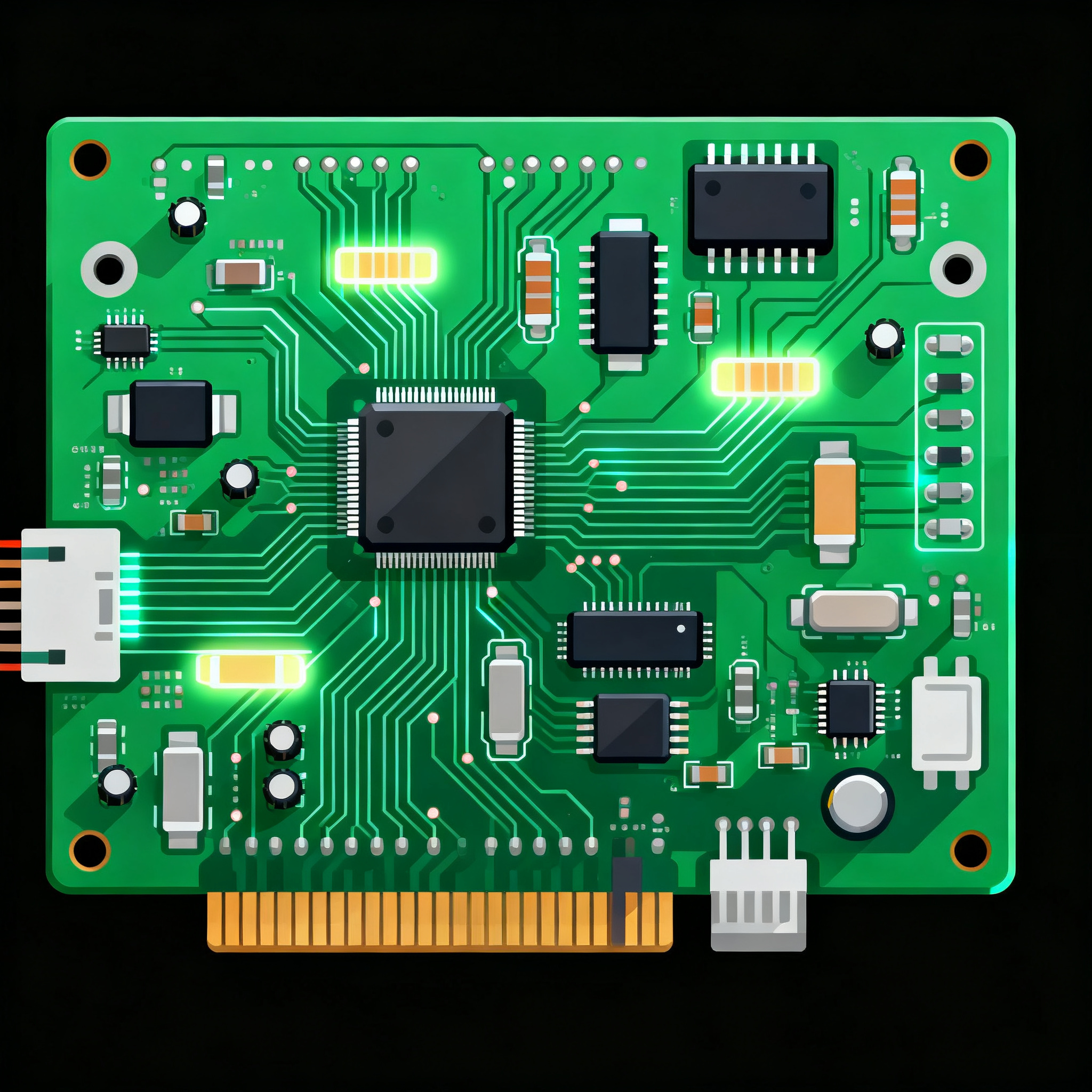
At the heart of every ADAS is a complex architecture that integrates various sensors, processors, and communication modules. The PCBA serves as a backbone, interconnecting these components to ensure seamless data flow and processing. Key architectural considerations include signal integrity, power distribution, and thermal management. Signal integrity is vital to prevent data corruption, while efficient power distribution ensures all components operate within specified limits. Additionally, thermal management is crucial to prevent overheating, which could lead to system failures. Engineers must also account for electromagnetic interference (EMI) and electromagnetic compatibility (EMC) to ensure the system functions correctly within the vehicle's environment.
Detailed Specifications
In designing PCBAs for ADAS, certain specifications are paramount to ensure the board's reliability and performance. These include trace width, spacing, via sizes, and clearances. Adhering to these specifications helps mitigate risks such as short circuits, signal loss, and overheating, which can compromise the system's integrity. Below is an overview of these critical design rules.
| Design Parameter | Minimum Value | Recommended Value |
|---|---|---|
| Trace Width | 0.1 mm | 0.2 mm |
| Trace Spacing | 0.1 mm | 0.2 mm |
| Via Diameter | 0.3 mm | 0.5 mm |
| Via Pad Size | 0.6 mm | 0.8 mm |
| Clearance to Edge | 0.3 mm | 0.5 mm |
| Minimum Hole Size | 0.2 mm | 0.3 mm |
| Annular Ring | 0.1 mm | 0.15 mm |
| Silkscreen Clearance | 0.1 mm | 0.2 mm |
| Solder Mask Clearance | 0.05 mm | 0.1 mm |
| Aspect Ratio | 6:1 | 8:1 |
| Board Thickness | 1.0 mm | 1.6 mm |
| Impedance Control | ±10% | ±5% |
Key Takeaways from the Specifications
The design parameters outlined in the table are foundational for ensuring the reliability and functionality of a PCBA in an ADAS context. For instance, trace width and spacing are crucial for carrying adequate current and minimizing crosstalk between signals. The via sizes and pad dimensions are essential for ensuring mechanical stability and electrical connectivity. Maintaining a proper clearance to the board edge prevents short circuits, while the specified aspect ratio ensures robust drilling processes. Engineers should meticulously adhere to these guidelines to optimize the performance and reliability of their PCB designs.
| Layer Configuration | Signal Layers | Power/Ground Layers |
|---|---|---|
| 2-Layer Board | 2 | 0 |
| 4-Layer Board | 2 | 2 |
| 6-Layer Board | 4 | 2 |
| 8-Layer Board | 6 | 2 |
| 10-Layer Board | 8 | 2 |
| 12-Layer Board | 8 | 4 |
| 14-Layer Board | 10 | 4 |
| 16-Layer Board | 12 | 4 |
Practical Implications
Layer stackup is a critical aspect of PCB design, particularly for high-performance applications like ADAS. A 4-layer board is often sufficient for basic applications, providing separate layers for power and ground to enhance signal integrity. However, as complexity increases, more layers are required to accommodate additional signal paths and power distribution networks. A 12-layer board, for example, offers enhanced flexibility for routing complex signal nets while maintaining robust power and ground planes. Engineers must balance the need for additional layers with cost considerations, as more layers typically increase fabrication costs.
| Material | Dielectric Constant (Dk) | Loss Tangent (Df) |
|---|---|---|
| FR-4 | 4.5 | 0.02 |
| Rogers 4350B | 3.48 | 0.0037 |
| Rogers 4003C | 3.38 | 0.0027 |
| Isola 370HR | 4.04 | 0.019 |
| Nelco N7000-2 | 3.7 | 0.015 |
| Taconic RF-35 | 3.5 | 0.0018 |
| Arlon 85N | 3.5 | 0.004 |
| Polyimide | 4.2 | 0.015 |
| PTFE | 2.1 | 0.0002 |
| Getek | 3.8 | 0.003 |
Application Guidelines
Choosing the right material for a PCB is vital for achieving desired electrical performance and reliability. FR-4 is a common choice due to its cost-effectiveness and satisfactory performance for many applications. However, for high-frequency applications, materials like Rogers 4350B or Taconic RF-35 offer lower loss tangents, which are crucial for maintaining signal integrity. Polyimide and PTFE materials are suitable for high-temperature applications due to their thermal stability. Engineers must evaluate the specific requirements of their ADAS project, including frequency, temperature, and environmental conditions, to select the most appropriate material.
Design Considerations
Effective PCB design for ADAS systems involves several key considerations to ensure optimal performance and reliability. Signal integrity is a top priority, requiring careful attention to trace impedance, crosstalk, and reflections. Utilizing controlled impedance traces and differential pair routing can mitigate these issues. Power integrity is equally important, necessitating robust power distribution networks and decoupling strategies to minimize voltage fluctuations. Thermal management is another critical consideration, as high-power components can generate significant heat. Implementing thermal vias, heat sinks, and proper component placement can help dissipate heat efficiently. Additionally, adhering to EMC guidelines is essential to prevent interference with other vehicle systems.
Step-by-Step Implementation
- Define System Requirements: Outline the specific ADAS features and performance criteria, including sensor types, data processing needs, and communication protocols.
- Develop Schematic Design: Create a detailed schematic, incorporating all necessary components and connectivity, while considering power and signal paths.
- Select Appropriate Components: Choose components that meet performance, size, and cost requirements, ensuring compatibility with the overall system design.
- Design PCB Layout: Implement the layout based on schematic design, adhering to design rules for trace width, spacing, and via sizes to ensure signal integrity and reliability.
- Perform Signal Integrity Analysis: Use simulation tools to analyze signal paths, identifying potential issues such as crosstalk and reflections, and make necessary adjustments.
- Prototype and Test: Fabricate a prototype board, conduct thorough testing to validate performance against initial requirements, and identify any necessary design modifications.
- Iterate Design: Refine the PCB design based on testing results, addressing any identified issues, and optimizing for manufacturability and cost-effectiveness.
- Finalize and Document: Complete final design adjustments, generate comprehensive documentation, including schematics, layout files, and assembly instructions, to facilitate manufacturing and assembly.
Common Issues & Solutions
- Signal Crosstalk: Use differential pairs and increase trace spacing to reduce undesired coupling between signals.
- Power Integrity Problems: Implement robust decoupling strategies and optimize power plane design to minimize voltage ripple.
- Thermal Management Challenges: Utilize thermal vias and strategically place heat sinks to enhance heat dissipation.
- EMI/EMC Violations: Incorporate shielding and filtering techniques to mitigate electromagnetic interference and ensure compliance.
- Manufacturing Defects: Adhere to IPC standards for PCB design and assembly to reduce the likelihood of defects such as solder bridges and misalignments.
- Component Placement Issues: Optimize component placement for signal flow, thermal management, and ease of assembly, avoiding high-density areas where possible.
Applications & Use Cases
ADAS systems are employed in various automotive applications, enhancing safety and convenience. Examples include adaptive cruise control systems that automatically adjust speed based on traffic conditions, lane departure warning systems that alert drivers when they unintentionally drift out of their lane, and collision avoidance systems that detect potential obstacles and apply brakes if necessary. These systems rely on precise PCB designs to ensure accurate sensor data processing and reliable communication with other vehicle systems.
Selection & Sourcing Guide
For sourcing components and materials for ADAS PCBAs, engineers can explore resources such as IC Online for a wide selection of electronic components. It's critical to collaborate with reputable suppliers who offer quality components that meet automotive standards, ensuring reliability and performance in demanding conditions.
FAQ
- What is the importance of trace width in PCB design? Trace width is crucial for carrying the necessary current without overheating and for maintaining signal integrity, particularly in high-frequency applications.
- How does layer stackup affect signal integrity? Proper layer stackup, with dedicated power and ground planes, reduces electromagnetic interference and enhances signal integrity by providing a stable reference plane.
- Why is material selection important for ADAS PCBAs? Material properties, such as dielectric constant and loss tangent, influence signal speed and integrity, especially in high-frequency applications, making the right choice critical for performance.
- How can I mitigate EMI in my PCB design? Implementing proper grounding, using shielding techniques, and maintaining adequate trace spacing can significantly reduce electromagnetic interference.
- What are the common manufacturing challenges for ADAS PCBAs? Common challenges include maintaining tight tolerances, ensuring high-quality solder joints, and preventing defects such as solder bridges and misalignments.
- How does thermal management impact ADAS PCB design? Effective thermal management prevents overheating, which can lead to component failure and reduced system reliability, making it a critical design consideration.
- What role does IPC standards play in PCB design? IPC standards provide guidelines for design, assembly, and quality inspection, ensuring consistency and reliability across PCB manufacturing processes.
- How do I ensure my PCB design is manufacturable? Collaborate with manufacturers early in the design process, adhere to design for manufacturability (DFM) principles, and follow industry standards to optimize the design for production.
- What testing is required for ADAS PCBAs? Comprehensive testing, including functional, thermal, and environmental tests, is necessary to validate the design and ensure it meets performance and safety requirements.
- How can I improve the reliability of my ADAS PCBA? Implementing robust design practices, selecting high-quality materials, and adhering to industry standards can enhance the reliability and longevity of the PCBA.
Conclusion
The design and implementation of PCBAs for Advanced Driver Assistance Systems require a thorough understanding of PCB design principles, material properties, and manufacturing considerations. By adhering to established design rules, selecting appropriate materials, and following best practices for signal integrity and thermal management, engineers can develop robust and reliable systems. As ADAS technology continues to evolve, staying informed about the latest standards and innovations will be key to success in this dynamic field.