Troubleshooting Common PCBA Soldering Defects: A Practical Guide for Engineers
Troubleshooting Common PCBA Soldering Defects: A Practical Guide for Engineers Introduction In the fast-paced world of electronics manufacturing, Printed Circuit Board Assemblies (PCBA) form the backb...
Introduction
In the fast-paced world of electronics manufacturing, Printed Circuit Board Assemblies (PCBA) form the backbone of any electronic device. Ensuring the quality and reliability of these assemblies is crucial, especially as devices become more complex and demand for high-performance components grows. Soldering defects in PCBA can lead to failures and significant financial losses. This guide focuses on understanding and addressing these common soldering defects, offering engineers practical insights and solutions to enhance the quality of their products.
Technical Overview
PCBA soldering involves attaching electronic components to a PCB using solder. The process is critical as it impacts the electrical connectivity and mechanical stability of the assembly. The core architecture of a PCBA includes layers of copper laminated onto a non-conductive substrate, with components soldered onto these layers. Key principles involve precise temperature control, component placement, and adherence to industry standards such as IPC-A-610, which outlines acceptability criteria for electronic assemblies. Understanding these principles is essential for troubleshooting and preventing soldering defects.
Detailed Specifications
When dealing with soldering defects, understanding the specifications of the integrated circuits (ICs) used in PCBA is crucial. Specifications like CPU speed, memory type, and power requirements influence the soldering process and the overall performance of the assembly. Here, we present core specifications of a typical IC component used in PCBA.
| Specification | Description | Value |
|---|---|---|
| CPU Speed | Maximum operating frequency of the IC | 3.2 GHz |
| Memory | Type and size of onboard memory | DDR4, 16GB |
| Peripherals | Supported interfaces and peripherals | USB, Ethernet, I2C |
| Power Supply | Voltage and current requirements | 5V, 2A |
| Package Type | Physical packaging of the IC | LGA |
| Temperature Range | Operational temperature range | -40°C to 85°C |
| Pin Count | Total number of pins | 256 |
| Die Size | Dimensions of the IC die | 10mm x 10mm |
| Manufacturing Process | Technology node used in fabrication | 7nm |
| Clock Multiplier | Internal clock frequency scaling | 32x |
Key Takeaways from the Specifications
The specifications listed above provide a comprehensive overview of the IC's capabilities and requirements. Understanding CPU speed and memory type is crucial for ensuring compatibility with other components and meeting performance expectations. The power supply specifications help in designing appropriate power delivery networks on the PCB. Additionally, the package type and pin count influence the soldering process, as they dictate the layout and spacing on the board. These factors must be carefully considered during the design and assembly phases to prevent defects like overheating or misalignment.
| Characteristic | Description | Value |
|---|---|---|
| Operating Voltage | Nominal voltage for operation | 1.2V |
| Max Current | Maximum current draw | 1.5A |
| Input High Voltage | Minimum voltage recognized as high | 2.0V |
| Input Low Voltage | Maximum voltage recognized as low | 0.8V |
| Output High Voltage | Minimum output voltage in high state | 3.3V |
| Output Low Voltage | Maximum output voltage in low state | 0.2V |
| Propagation Delay | Time for signal propagation | 5ns |
| Rise Time | Time for signal to rise | 2ns |
| Fall Time | Time for signal to fall | 2ns |
| Leakage Current | Current leakage in off state | 5µA |
| Power Dissipation | Heat generated during operation | 500mW |
| Thermal Resistance | Resistance to heat flow | 20°C/W |
Practical Implications
The electrical characteristics outlined in the table are vital for ensuring the IC functions correctly within the PCBA. Operating voltage and current specifications are critical for power supply design, ensuring adequate voltage levels without overloading the circuit. Timing specifications like propagation delay and rise/fall times affect signal integrity, crucial in high-speed applications. Understanding these parameters helps in designing circuits that minimize power dissipation and prevent overheating, which are common causes of soldering defects.
| Use Case | Configuration | Description |
|---|---|---|
| Consumer Electronics | Standard Configuration | Basic setup for everyday devices |
| Industrial Automation | Rugged Configuration | Enhanced durability and reliability |
| Automotive Systems | High-Temperature Configuration | Operates under extreme conditions |
| Telecommunications | High-Frequency Configuration | Supports high-speed data transfer |
| Medical Devices | Low-Power Configuration | Optimized for energy efficiency |
| IoT Devices | Compact Configuration | Miniaturized for space constraints |
| Aerospace Systems | Radiation-Hardened Configuration | Withstands harsh environments |
| Wearable Technology | Flexible Configuration | Adapts to body contours and movement |
Application Guidelines
The application table highlights various configurations of ICs tailored for specific use cases. Each application demands unique considerations; for instance, automotive systems require high-temperature configurations to function reliably under extreme conditions, while IoT devices prioritize compact and energy-efficient designs. Understanding these configurations aids engineers in selecting the right ICs for their projects, ensuring optimal performance and longevity in the intended application environment.
Design Considerations
Designing a PCBA involves several critical considerations to minimize soldering defects and ensure reliable performance. Adhering to IPC standards, such as IPC-2221 for design and IPC-A-610 for assembly, provides a robust framework for quality assurance. Engineers must focus on the following key areas:
- Component Placement: Proper alignment and spacing of components prevent bridging and ensure appropriate heat dissipation.
- Solder Paste Application: Uniform deposition of solder paste is crucial for achieving good solder joints. Use of stencils and controlled application methods is recommended.
- Reflow Profile: Establishing an optimal reflow temperature profile prevents overheating and ensures proper solder reflow.
- Thermal Management: Incorporating thermal vias and heatsinks helps in managing heat generated by high-power components.
- Board Design: Considerations like trace width, via placement, and layer stack-up influence the overall performance and reliability of the PCBA.
- Inspection and Testing: Implementing thorough inspection processes, such as Automated Optical Inspection (AOI), helps in early detection of defects.
By focusing on these design considerations, engineers can significantly reduce the occurrence of soldering defects and enhance the reliability of their PCBAs.
Step-by-Step Implementation
Implementing a robust PCBA design involves several steps, each requiring careful attention to detail:
- Define Requirements: Begin by clearly defining the specifications and requirements for the PCBA, considering the intended application and environment.
- Choose Components: Select suitable components based on electrical characteristics and application guidelines, ensuring compatibility and performance.
- Design Layout: Use PCB design software to create a layout that optimizes component placement and routing for signal integrity and thermal management.
- Create Schematic: Develop a detailed schematic capturing all connections and components, serving as a blueprint for the PCB layout.
- Generate Gerber Files: Produce Gerber files from the design software, which are essential for PCB fabrication.
- Prototype and Test: Fabricate a prototype of the PCBA and conduct rigorous testing to identify and rectify any issues.
- Iterate Design: Based on testing feedback, iterate the design to address any defects or performance concerns.
- Finalize and Produce: Once satisfied with the prototype, finalize the design and proceed with mass production, ensuring all quality standards are met.
Following these steps systematically ensures a well-designed and reliable PCBA, minimizing the risk of soldering defects and other issues.
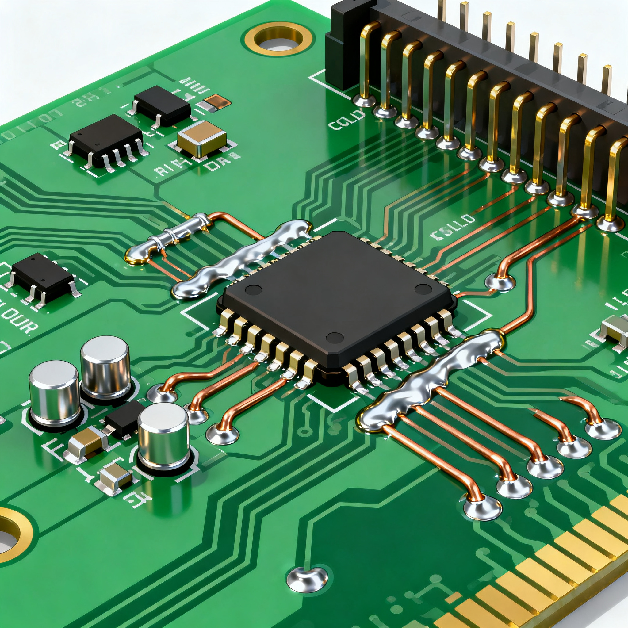
Common Issues & Solutions
Soldering defects can manifest in various forms, each requiring specific solutions:
- Bridging: Often caused by excessive solder paste or misalignment. Solution: Adjust stencil design and ensure precise component placement.
- Cold Joints: Result from inadequate heat during soldering. Solution: Optimize reflow temperature profiles and ensure even heat distribution.
- Voiding: Caused by trapped gas or flux during soldering. Solution: Use vacuum soldering techniques and adjust paste formulation.
- Insufficient Solder: Leads to weak joints. Solution: Ensure adequate solder paste volume and adjust stencil thickness.
- Non-Wetting: Occurs when solder does not adhere to the pad. Solution: Clean pads thoroughly and use appropriate flux.
- Component Tombstoning: Caused by uneven heating or solder volume. Solution: Adjust reflow profile and balance solder paste application.
Addressing these common issues with targeted solutions helps maintain the integrity and performance of the PCBA.
Applications & Use Cases
PCBAs are integral to various industries, each with unique demands:
- Consumer Electronics: Devices like smartphones and laptops rely on PCBAs for compact and efficient performance.
- Automotive Industry: PCBAs in vehicles manage critical functions like engine control and infotainment systems.
- Medical Devices: High-reliability PCBAs are crucial in life-saving equipment, requiring stringent quality standards.
- Telecommunications: High-frequency PCBAs enable rapid data transmission in communication networks.
- IoT Applications: PCBAs in IoT devices prioritize low power consumption and connectivity.
Understanding the specific requirements of each industry aids in selecting and designing the right PCBA solutions.
Selection & Sourcing Guide
Choosing the right components for PCBA involves careful evaluation of specifications and application needs. For sourcing, visit IC Online for a comprehensive selection of ICs and components, ensuring quality and compatibility with your design requirements.
FAQ
- What are the most common soldering defects in PCBA? Common defects include bridging, cold joints, voiding, insufficient solder, non-wetting, and tombstoning.
- How can I prevent bridging in PCBAs? Ensure precise component placement and adjust solder paste volume and stencil design.
- What is the role of reflow profile in soldering? The reflow profile ensures proper heating and cooling, preventing defects like cold joints and tombstoning.
- Why is component selection critical for PCBA? Components must meet electrical specifications and application requirements to ensure reliable performance.
- How do I test for soldering defects? Use inspection techniques like AOI, X-ray, and functional testing to identify and address defects.
- What standards should I follow for PCBA quality? Adhere to IPC standards such as IPC-A-610 for assembly and IPC-2221 for design.
- How does thermal management affect soldering? Proper thermal management prevents overheating and ensures reliable solder joints.
- What are the implications of voiding in solder joints? Voids can weaken joints and affect thermal and electrical performance.
- How do I optimize solder paste application? Use precision stencils and controlled application methods to ensure uniform solder deposition.
- What is the impact of environmental conditions on PCBA? Environmental factors like temperature and humidity can affect soldering quality and component performance.
Conclusion
Understanding and addressing soldering defects in PCBA is crucial for ensuring the reliability and performance of electronic devices. By focusing on detailed specifications, electrical characteristics, and application guidelines, engineers can make informed decisions in the design and manufacturing process. Adhering to industry standards and implementing robust testing and inspection procedures further enhances the quality of PCBAs, minimizing defects and maximizing operational efficiency.