Troubleshooting 6 Common Pitfalls in Satellite Communication PCB Assembly: From Outgassing to Thermal Mismatch
Why Satellite PCB Assemblies Fail Before They Even Leave the Cleanroom You can follow every rule in IPC-2221 and still produce a satellite PCB that fails within 72 hours of orbit insertion. The reason...
Why Satellite PCB Assemblies Fail Before They Even Leave the Cleanroom
You can follow every rule in IPC-2221 and still produce a satellite PCB that fails within 72 hours of orbit insertion. The reason is simple: terrestrial manufacturing standards were never designed for the triple threat of hard vacuum, thermal swings exceeding 200°C, and launch vibration loads that rattle every solder joint to its fatigue limit. A board that passes Class 3 inspection on the bench can outgas volatile compounds that condense on optical surfaces, fracture at the laminate-to-copper interface during the first eclipse cycle, or grow tin whiskers that bridge fine-pitch BGA pads in zero-gravity.
Satellite communication PCBs occupy a punishing intersection of RF performance requirements and survivability constraints. Your 28 GHz phased-array beamformer doesn't care that the board is cycling from -40°C to +125°C every 90 minutes in low Earth orbit — but the dielectric constant of your substrate certainly does, and a 0.5% shift in Dk can detune an entire antenna array. Meanwhile, the vacuum environment strips away convective cooling, turning every via into a potential hot spot and every material interface into a source of molecular contamination.
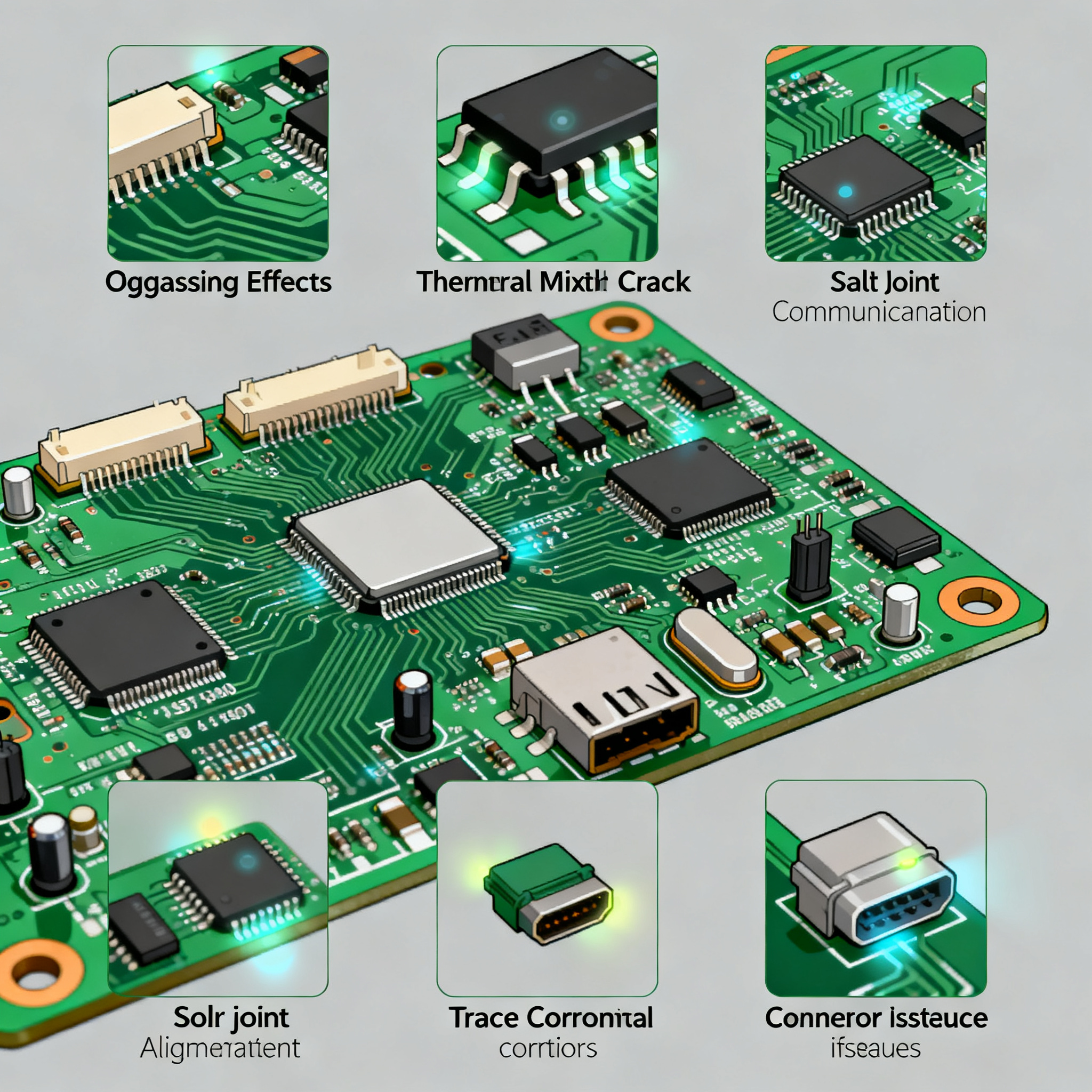
The six pitfalls we'll dissect — outgassing, CTE mismatch, tin whiskers, plating voids, contamination, and solder joint fatigue — share a common thread: they're all manageable if you catch them before the conformal coat goes on, and catastrophic if you discover them during thermal-vacuum qualification. This article walks through the physics behind each failure mode and the assembly-level countermeasures that separate flight-ready hardware from expensive scrap.
Key Takeaway: IPC Class 3 is the starting line for satellite PCB assembly, not the finish line. Space-grade reliability demands additional process controls — vacuum bake-out, CTE-matched material stacks, nickel-gold plating, and cleanroom protocols — that go well beyond standard high-reliability manufacturing.
Outgassing, CTE Mismatch, and the Physics Behind the Six Silent Killers
Outgassing is the release of trapped volatiles — moisture, solvents, plasticizers, and uncured resin fractions — when a material is exposed to vacuum and elevated temperature. The standard metric comes from ASTM E595: Total Mass Loss (TML) must be ≤1.0% and Collected Volatile Condensable Material (CVCM) ≤0.1% for most space applications. These numbers aren't arbitrary. A single FR-4 board with 2.5% TML can deposit enough condensable film on a satellite's star tracker lens to degrade attitude determination accuracy by several arcseconds — a mission-killing failure for a communications satellite that relies on precise pointing.
CTE mismatch is the second killer, and it operates on a different timescale. Where outgassing damage accumulates gradually, thermal mismatch stress is cyclic and cumulative. Your PCB laminate expands at 14–17 ppm/°C (typical FR-4 in the X-Y plane) while the ceramic BGA package on top expands at 6–7 ppm/°C. Over 5,000 thermal cycles — roughly one year in LEO — that delta translates into shear strain at every solder ball. The math is unforgiving: strain per cycle multiplied by cycle count eventually exceeds the fatigue ductility of SAC305 solder, and cracks initiate at the package corners where the distance from neutral point is greatest.
Then there are the four other mechanisms that don't get the same attention as outgassing and CTE but kill just as effectively. Tin whiskers — single-crystal filaments that grow spontaneously from pure tin surfaces — can reach lengths of several millimeters in vacuum, where the absence of an oxide-inhibiting atmosphere accelerates growth. Plating voids in via barrels create stress concentrators that become crack initiation sites during thermal cycling. Ionic contamination from flux residues or handling creates electrochemical migration paths that lower surface insulation resistance. And solder joint fatigue, while partly driven by CTE mismatch, has its own aggravating factors including voiding, intermetallic growth, and inadequate standoff height.
The table below compares outgassing and CTE characteristics for the four substrate families most commonly considered for satellite communication PCBs:
| Substrate Material | Typical TML (%) | Typical CVCM (%) | CTE X-Y (ppm/°C) | CTE Z (ppm/°C) | Tg (°C) | Dk @ 10 GHz |
|---|---|---|---|---|---|---|
| Standard FR-4 | 0.8–2.5 | 0.05–0.25 | 14–17 | 50–70 | 130–140 | 4.2–4.6 |
| Low-Outgassing FR-4 | 0.3–0.8 | 0.02–0.08 | 12–15 | 40–55 | 150–170 | 3.8–4.2 |
| Polyimide | 0.1–0.5 | 0.01–0.05 | 12–14 | 45–60 | 250–260 | 3.5–3.8 |
| Ceramic (Alumina/AlN) | <0.05 | <0.01 | 4–7 | 4–7 | N/A | 8.5–10.0 |
| PTFE-Based (Rogers RO4000) | 0.05–0.2 | 0.01–0.03 | 10–16 | 24–40 | >280 | 3.3–3.5 |
What jumps out from this data is the trade-off between RF performance and mechanical robustness. Ceramic substrates offer near-zero outgassing and CTE that matches silicon and GaAs die almost perfectly — but their high dielectric constant limits impedance-controlled trace geometries and increases insertion loss at millimeter-wave frequencies. PTFE-based laminates deliver the lowest loss tangent and most stable Dk across temperature, but their high Z-axis CTE creates reliability risks for plated through-holes. Polyimide splits the difference with moderate outgassing, acceptable RF properties, and a glass transition temperature high enough to survive lead-free soldering without delamination.
Note: The Z-axis CTE is particularly critical for plated through-hole reliability. When the laminate expands vertically at 50–70 ppm/°C while the copper barrel expands at only 17 ppm/°C, the resulting strain concentrates at the barrel-to-pad interface — exactly where most PTH failures initiate during thermal cycling.
Polyimide vs. Ceramic vs. Low-Outgassing FR-4: Which Substrate Survives the Vacuum of Space?
Choosing a substrate for satellite communication PCBs means navigating a three-way tug-of-war between outgassing compliance, RF performance, and manufacturing practicality. The decision tree starts with mission duration and environmental severity. A 90-day CubeSat in a 600 km orbit faces roughly 1,400 thermal cycles; a 15-year geostationary communications satellite sees slower but deeper cycles and far more stringent contamination requirements because its optical payloads and solar arrays must maintain efficiency for decades.
Low-outgassing FR-4 variants — often based on phenolic-cured epoxy systems with reduced free-epoxy content — can meet ASTM E595 thresholds after vacuum bake-out. They're attractive for cost-constrained programs because they run on standard PCB fabrication lines with minimal process modification. But the margin is thin. A lot of laminate that passes TML at 0.8% in the supplier's test coupon can exceed 1.0% on a production board with higher resin content in the weave-rich areas. And even when outgassing is controlled, the CTE mismatch with ceramic packages remains a reliability limiter for high-cycle-count missions.
Polyimide laminates — often specified as polyimide/aramid or pure polyimide systems — raise the glass transition temperature to 250°C or higher, which buys you two things: resistance to delamination during multiple reflow cycles, and a broader temperature window where the CTE remains stable. For LEO constellations where boards may see 15,000 cycles over five years, that stability translates directly into solder joint fatigue life. The trade-off is cost: polyimide materials typically run 3–5× the price of FR-4, and they require more aggressive desmear and metallization processes for reliable via plating.
Ceramic substrates — primarily 96% or 99.6% alumina, with aluminum nitride for high-thermal-dissipation applications — are the gold standard for outgassing and CTE matching. Their TML is essentially unmeasurable by standard ASTM E595 procedures, and their CTE of 6–7 ppm/°C aligns with the alumina and silicon die they host. The catch is manufacturability: ceramic PCBs are limited in layer count (typically 4–8 layers maximum), require thick-film or thin-film metallization rather than electroplated copper, and cost 10–20× more than equivalent polyimide boards. They're reserved for high-power amplifiers, switch matrices, and other RF front-end functions where thermal conductivity and dimensional stability are non-negotiable.
PTFE-based laminates like Rogers RO4350B and RO4003C occupy a specialized niche for millimeter-wave satellite communication circuits — phased-array feed networks, Wilkinson dividers, and coupled-line filters above 20 GHz. Their low and stable dielectric constant enables precise impedance control, but their Z-axis CTE demands careful via design: larger annular rings, ductile copper plating, and sometimes conductive epoxy fill to relieve barrel stress. Nova PCBA's material selection guidance helps engineering teams weigh these trade-offs against mission requirements, avoiding the common trap of over-specifying an expensive ceramic substrate when a properly processed polyimide board would meet all reliability targets.
The comparison matrix below captures the decision factors at a glance:
| Comparison Metric | Low-Outgassing FR-4 | Polyimide | Ceramic (Alumina) | Selection Criteria & Failure Boundary |
|---|---|---|---|---|
| Outgassing Margin (TML) | 0.3–0.8% (narrow margin) | 0.1–0.5% (comfortable) | <0.05% (essentially zero) | Choose polyimide or ceramic if CVCM margin <2× requirement |
| CTE Match to Ceramic BGA | Poor (delta 8–10 ppm/°C) | Moderate (delta 5–7 ppm/°C) | Excellent (delta <2 ppm/°C) | Underfill required for FR-4; ceramic eliminates need |
| RF Performance @ 30 GHz | Marginal (Df ~0.020) | Good (Df ~0.008–0.012) | Poor (Dk too high for 50Ω lines) | PTFE-based preferred above 20 GHz |
| Max Layer Count | 24+ | 16–20 | 4–8 | High-layer-count digital boards favor FR-4 or polyimide |
| Relative Cost (per sq. in.) | 1× (baseline) | 3–5× | 10–20× | Mission duration justifies material investment |
| Thermal Conductivity (W/m·K) | 0.3–0.4 | 0.2–0.3 | 20–170 (AlN) | High-power RF needs ceramic or metal-core |
The selection boundary is rarely absolute. Many satellite communication payloads use hybrid construction: a polyimide digital processing board married to a ceramic power amplifier substrate, connected by a flex circuit that absorbs differential expansion. The key is recognizing that no single material solves all six pitfalls — and that the assembly process must be tuned to the specific vulnerabilities of whichever substrate you choose.
From Bake-Out to Via-in-Pad: Six Assembly Fixes That Stop Outgassing, Warpage, and Solder Fractures
Each of the six failure mechanisms has a corresponding assembly-level countermeasure. The table below maps pitfall to fix, with process parameters validated across multiple satellite programs:
| Pitfall | Assembly Fix | Process Parameters | Verification Method |
|---|---|---|---|
| Outgassing | Vacuum bake-out before conformal coat | 125°C, <10⁻³ Torr, 24–48 hours; ramp <5°C/min to avoid delamination | ASTM E595 on witness coupons; TML and CVCM within spec |
| CTE Mismatch / Warpage | Symmetric stackup + CTE-matched bonding | Even layer count; copper balance >70% per layer; bondply CTE within 3 ppm/°C of core | Shadow moiré at 25°C, 100°C, and -40°C; warpage <0.5% diagonal |
| Tin Whiskers | Nickel-gold (ENIG) or Ni-Pd-Au plating | ENIG: 3–6 μm Ni, 0.05–0.12 μm Au; avoid pure tin finishes entirely | XRF thickness verification; whisker growth testing per JESD22-A121 |
| Plating Voids | Via-in-pad with filled and capped vias | Conductive or non-conductive epoxy fill; planarization to <15 μm depression; cap plating 15–25 μm Cu | Cross-section microscopy; 100% via inspection on flight boards |
| Contamination | Class 100 (ISO 5) cleanroom assembly | Ionic contamination <1.56 μg/cm² NaCl equivalent; no-clean flux with SIR >100 MΩ after 168 hours at 85°C/85% RH | ROSE testing; ion chromatography on first-article assemblies |
| Solder Joint Fatigue | Strain-relief underfill + standoff height control | Underfill Tg >130°C, CTE 20–30 ppm/°C; standoff 75–125 μm for BGAs; solder volume per IPC-A-610 Class 3 | Thermal cycling -55°C to +125°C, 500 cycles minimum; dye-and-pry after cycling |
Vacuum bake-out deserves special emphasis because it's the single most effective — and most frequently skipped — process step for outgassing control. The physics is straightforward: elevated temperature increases the diffusion rate of trapped volatiles, and low pressure creates a concentration gradient that pulls them out of the laminate. But the execution matters. Ramp too fast and you'll delaminate the board as internal vapor pressure exceeds the resin's cohesive strength. Bake too short and you'll leave enough residual moisture to fail TML by a fraction of a percent. The 24–48 hour window at 125°C is a proven sweet spot for polyimide and low-outgassing FR-4; PTFE-based laminates can tolerate higher temperatures but rarely need them given their inherently low outgassing.
Symmetric stackup design is your primary defense against warpage-driven solder fractures. The principle is simple: every layer of prepreg, core, and copper on one side of the board's neutral axis must have a mirror-image counterpart on the other side. In practice, this means even layer counts, balanced copper distribution (aim for >70% copper coverage symmetry), and careful attention to the resin content of bonding layers. A board that measures 0.2% warpage at room temperature can exceed 1.5% at -40°C if the stackup is asymmetric — and 1.5% warpage across a 200 mm board puts enough tensile stress on corner BGA balls to cause cracking within the first hundred thermal cycles.
ENIG plating has become the de facto standard for satellite PCB surface finishes because it solves two problems simultaneously: it provides a flat, solderable pad surface for fine-pitch components, and the nickel barrier layer eliminates the tin whisker risk that haunts pure tin and immersion tin finishes. The gold thickness is critical — too thin (<0.05 μm) and the nickel oxidizes through pinholes; too thick (>0.12 μm) and the gold embrittles the solder joint. For satellite applications where boards may be stored for months before flight, the thicker end of the range (0.08–0.12 μm) provides better shelf-life protection.
Via-in-pad with filled vias addresses plating voids at their root cause: the difficulty of achieving uniform copper deposition in high-aspect-ratio holes. When a via is placed in a BGA pad, any void in the barrel creates a stress concentration that becomes the initiation point for a barrel crack. Filling the via with conductive or non-conductive epoxy and then planarizing and capping with copper eliminates the void entirely, distributing mechanical stress across a solid column rather than a hollow tube. The added cost — roughly 15–25% per board — is trivial compared to the cost of a solder joint failure on orbit.
Cleanroom discipline extends beyond particle counts. Ionic contamination from flux residues, fingerprint salts, and even outgassed plasticizers from assembly fixtures can reduce surface insulation resistance below the 100 MΩ threshold that high-impedance RF circuits demand. The 1.56 μg/cm² NaCl equivalent limit comes from long-standing military and aerospace cleanliness standards, and it's verified through Resistivity of Solvent Extract (ROSE) testing on every production lot. IPC-A-610 Class 3 inspection criteria provide the visual acceptance framework, but ionic cleanliness requires chemical verification that goes beyond visual inspection.
Underfill application is the last line of defense against CTE-driven solder fatigue. By bonding the component package to the PCB surface with a filled epoxy that has a CTE intermediate between the two, underfill distributes shear strain across the entire bonded area rather than concentrating it in the solder balls. The underfill's glass transition temperature must exceed the maximum operating temperature of the board — otherwise the underfill itself becomes a source of expansion mismatch above Tg. For LEO satellites that cycle from -40°C to +125°C, an underfill with Tg >130°C provides a comfortable margin.
Satellite PCB Assembly Pitfalls: What Senior Engineers and Buyers Ask
Q: What outgassing specifications should I require for satellite PCB materials, and how do I verify compliance?
Specify ASTM E595 with Total Mass Loss (TML) ≤1.0% and Collected Volatile Condensable Material (CVCM) ≤0.1% as your baseline. For optics-adjacent or cryogenic applications, tighten to TML ≤0.5% and CVCM ≤0.05%. Request material test reports directly from laminate suppliers — every qualified aerospace laminate comes with lot-specific E595 data. Don't rely solely on supplier certificates; perform pre-bake verification on first-article assemblies by placing witness coupons in your vacuum oven alongside the flight boards and sending them to an independent lab for post-bake E595 testing. The difference between supplier TML and post-assembly TML can reveal contamination introduced during fabrication that would otherwise go undetected.
Q: How does CTE mismatch actually cause solder joint failure in LEO satellites, and what design rules mitigate it?
Repeated thermal cycling from -40°C to +125°C — the typical range for LEO satellites passing through eclipse — shears solder joints when the PCB's coefficient of thermal expansion differs from that of the component packages mounted on it. The shear strain per cycle is proportional to the CTE difference multiplied by the distance from the package's neutral point, which is why corner balls fail first. Over 5,000 to 15,000 cycles (one to five years in LEO), the accumulated plastic strain exceeds the fatigue ductility of the solder alloy. Mitigation starts with CTE-matched laminates: polyimide (12–14 ppm/°C) or ceramic-filled hydrocarbon (10–12 ppm/°C) bring the board closer to the 6–7 ppm/°C of ceramic packages. Symmetric stackups prevent warpage from amplifying local strain. And strain-relief underfills with CTE of 20–30 ppm/°C and Tg above 130°C distribute shear stress across the entire bonded interface rather than concentrating it in solder joints.
Q: Is it ever acceptable to use standard FR-4 for a non-critical satellite subsystem, and what additional processes are needed?
Only for short-duration, low-cost missions — think university CubeSats with 90-day operational lifetimes and no sensitive optical payloads — and even then, only with aggressive risk mitigation. The board must undergo a thorough vacuum bake-out (125°C, <10⁻³ Torr, minimum 48 hours) to drive off volatiles. A conformal coating — typically parylene or silicone-based — must be applied after bake-out to trap any residual outgassing and provide a moisture barrier. And the program must accept that outgassing may still contaminate adjacent optics, star trackers, or thermal control surfaces. Most professional satellite programs avoid standard FR-4 entirely; the cost savings of a $200 laminate are dwarfed by the $50,000+ cost of a thermal-vacuum qualification failure. Low-outgassing FR-4 variants with phenolic-cured epoxy systems offer a middle ground at roughly 1.5–2× the material cost.
Q: What plating finish is safest for long-term reliability in vacuum — ENIG, HASL, or immersion silver?
ENIG (electroless nickel immersion gold) is the preferred finish for satellite PCBs. The nickel layer (3–6 μm) acts as a diffusion barrier that prevents copper migration and provides a flat, solderable surface that resists oxidation during extended storage. The immersion gold flash (0.05–0.12 μm) protects the nickel from passivation without introducing enough gold to cause embrittlement. Avoid immersion silver entirely for space applications — silver migrates under bias in the presence of moisture and sulfur, and creep corrosion can occur even in the cleanroom if boards are stored improperly. HASL (hot air solder leveling) is unsuitable for satellite boards because the uneven surface topography creates coplanarity problems for fine-pitch components, and the thermal shock of the HASL process can delaminate high-Tg laminates. For the highest reliability, some programs specify ENEPIG (electroless nickel, electroless palladium, immersion gold), which adds a palladium layer that eliminates the risk of nickel corrosion at the gold pinholes.
Q: How do I qualify a PCB assembly vendor for space-grade work, and what certifications should I look for?
Start with AS9100 certification — the aerospace-specific extension of ISO 9001 that includes risk management, configuration control, and counterfeit parts prevention requirements. Verify demonstrated IPC-A-610 Class 3 capability through process control documentation and first-article inspection reports, not just certificates on a wall. The vendor must have in-house vacuum bake-out capability (not subcontracted) with calibrated temperature and vacuum instrumentation, plus ionic cleanliness verification equipment (ROSE tester or ion chromatograph). Ask for evidence of completed satellite programs — flight heritage matters more than any certification. During an on-site audit, inspect their material traceability system (every laminate lot, solder paste batch, and plating chemistry must be traceable to the finished board), their contamination control protocols (including garment discipline, glove changes, and periodic surface particle counts), and their handling procedures for moisture-sensitive devices. A vendor who can't show you their bake-out logbooks and cleanliness records during the audit won't magically develop those disciplines for your program. Nova PCBA maintains these capabilities in-house, with documented processes for satellite-grade assembly that include vacuum bake-out, ENIG plating, via filling, and Class 100 cleanroom protocols.
References & Further Reading
- IPC — Association Connecting Electronics Industries — IPC-2221 (Generic Standard on Printed Board Design) and IPC-A-610 (Acceptability of Electronic Assemblies)
- ASTM E595 — Standard Test Method for Total Mass Loss and Collected Volatile Condensable Materials from Outgassing in a Vacuum Environment