Top PCB Prototype Suppliers: Evaluating Quality and Turnaround Time
Top PCB Prototype Suppliers: Evaluating Quality and Turnaround Time Introduction Printed Circuit Boards (PCBs) are the backbone of modern electronics, forming the foundational structure that supports ...
Introduction
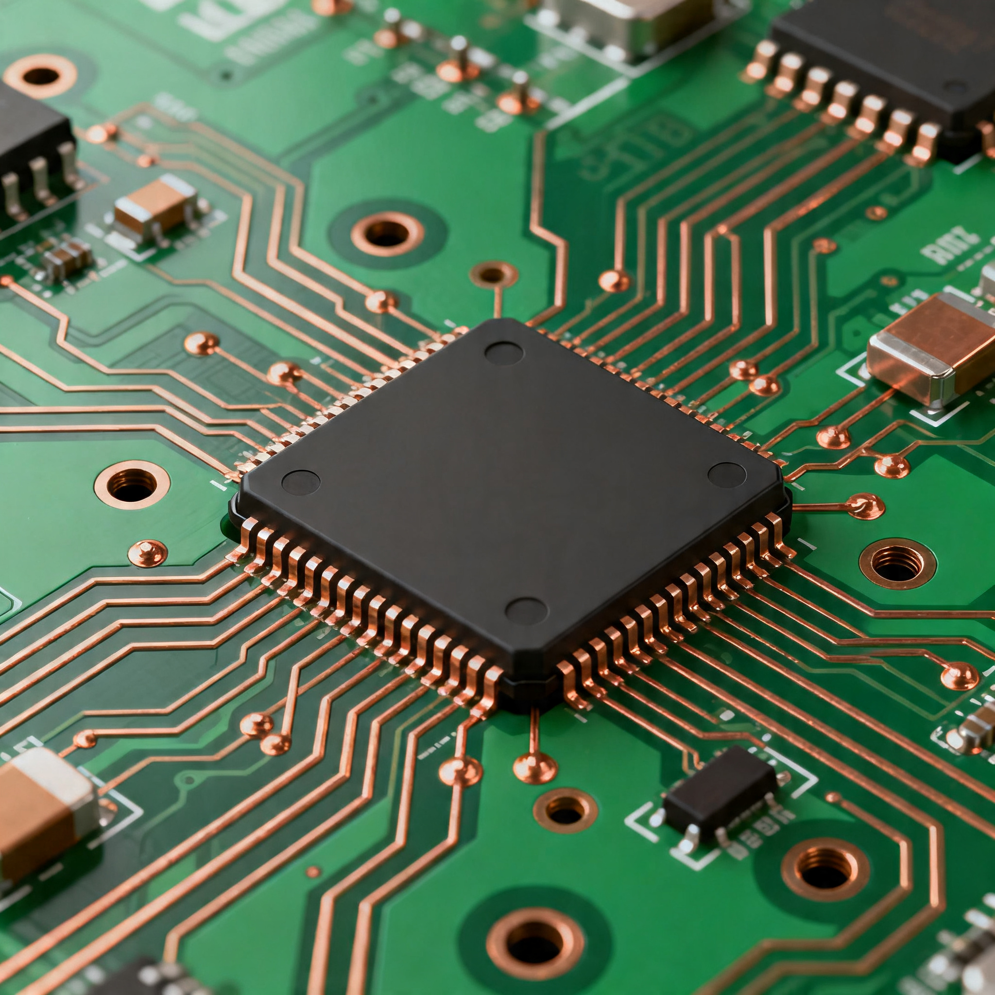
Printed Circuit Boards (PCBs) are the backbone of modern electronics, forming the foundational structure that supports and connects electronic components. With the rapid advancements in technology, the demand for high-quality PCB prototypes with quick turnaround times has never been greater. This article explores the critical aspects of PCB design, focusing on layout rules, stackup design, signal integrity, and manufacturing considerations, to help you choose the right prototype supplier.
Technical Overview
The design and manufacturing of PCBs involve a complex interplay of various technical aspects. Core concepts such as trace width, spacing, via sizes, and clearances play a significant role in ensuring signal integrity and preventing issues like crosstalk and electromagnetic interference. The architecture of a PCB design is further influenced by the layer stackup options, which affect the board's electrical performance and mechanical strength. Additionally, material properties such as dielectric constants and loss tangent determine the board's suitability for specific applications. Understanding these principles is crucial for optimizing PCB performance and manufacturability.
Detailed Specifications
In PCB design, specifications are critical for ensuring that the final product meets the desired performance and reliability standards. Factors such as trace width, spacing, and via sizes are essential in maintaining signal integrity and manufacturability. Let's delve into the specific design rules that are pivotal in PCB layout.
| Design Parameter | Standard Value | Importance |
|---|---|---|
| Trace Width | 0.2 mm | Ensures current carrying capacity |
| Trace Spacing | 0.2 mm | Prevents short circuits |
| Via Diameter | 0.6 mm | Allows interlayer connections |
| Annular Ring | 0.15 mm | Provides mechanical strength to vias |
| Clearance | 0.3 mm | Ensures isolation between traces |
| Pad Size | 0.5 mm | Supports component soldering |
| Drill Hole Size | 0.3 mm | For component leads |
| Aspect Ratio | 10:1 | Determines manufacturability of vias |
| Impedance Control | ±10% | Maintains signal integrity |
| Solder Mask Clearance | 0.1 mm | Prevents solder bridging |
| Minimum Feature Size | 0.1 mm | Defines manufacturable limits |
Key Takeaways from the Specifications
The design rules outlined in the table are critical for ensuring a reliable and functional PCB. Trace width and spacing are fundamental in preventing electrical shorts and supporting the required current flow. Via sizes and annular rings contribute to the mechanical integrity and electrical connectivity of the board. Understanding these parameters helps in optimizing the layout for manufacturability and performance, ensuring that the PCB meets the intended design criteria without compromising on quality.
| Layer Configuration | Description | Applications |
|---|---|---|
| Single Layer | One conductive layer | Simple electronics, low cost |
| Double Layer | Two conductive layers | Basic consumer electronics |
| 4-Layer Stackup | Two signal layers, two ground/power planes | Improved signal integrity |
| 6-Layer Stackup | Four signal layers, two ground/power planes | High-speed applications |
| 8-Layer Stackup | Six signal layers, two ground/power planes | Complex, high-density designs |
| Rigid-Flex | Combination of rigid and flexible layers | Wearable and compact devices |
| HDI (High-Density Interconnect) | Microvias, finer lines | Smartphones, tablets |
Practical Implications
The choice of layer stackup has significant implications for the PCB's performance and cost. A single or double-layer board may suffice for simple applications, but more complex designs benefit from multi-layer configurations. For instance, a 4-layer stackup offers better signal integrity by providing dedicated ground and power planes, while an 8-layer stackup is ideal for high-density and high-speed applications. Selecting the appropriate stackup ensures optimal electrical performance and mechanical stability, tailored to the specific needs of the application.
| Material | Dielectric Constant (Dk) | Loss Tangent (Df) |
|---|---|---|
| FR-4 | 4.5 | 0.02 |
| Rogers 4350B | 3.48 | 0.0037 |
| Rogers 4003C | 3.38 | 0.0027 |
| PTFE (Teflon) | 2.1 | 0.001 |
| Polyimide | 4.2 | 0.004 |
| Isola FR408HR | 3.66 | 0.009 |
| Nelco N7000-2 | 3.7 | 0.0023 |
| Arlon 85N | 3.5 | 0.0035 |
| Megtron 6 | 3.2 | 0.002 |
Application Guidelines
Material properties such as dielectric constant and loss tangent are critical for selecting the right substrate for your PCB. FR-4 is a common choice for general-purpose applications due to its balanced properties. However, for high-frequency applications, materials like Rogers 4350B or PTFE offer lower dielectric constants and loss tangents, minimizing signal loss and distortion. Understanding these properties helps in choosing materials that align with the performance requirements and environmental conditions of the application, ensuring reliability and efficiency.
Design Considerations
Designing a PCB involves several considerations to ensure performance and manufacturability. Signal integrity is paramount, requiring careful attention to trace impedance, crosstalk, and EMI. Ground and power plane design must support adequate current flow and minimize loop areas. Thermal management is another critical aspect, often addressed through strategic placement of vias and heat sinks. Additionally, manufacturability concerns such as minimum trace width, spacing, and aspect ratios need to be balanced with the electrical requirements. By adhering to industry standards and best practices, designers can create robust and reliable PCB layouts that meet the intended specifications.
Step-by-Step Implementation
- Define Requirements: Begin by understanding the electrical and mechanical requirements of your design. This includes power levels, signal types, and environmental conditions.
- Schematic Design: Create a detailed schematic that outlines the electrical connections and component layout. Use design software tools for accuracy and efficiency.
- Component Placement: Strategically place components on the board to minimize trace lengths and optimize thermal performance. Ensure that sensitive components are adequately shielded.
- Routing: Route traces to connect the components, adhering to design rules for trace width, spacing, and via sizes. Pay attention to signal integrity and impedance control.
- Layer Stackup Design: Choose an appropriate layer stackup based on the complexity and performance requirements of your design. Consider the need for power and ground planes.
- Validation and Testing: Perform Design Rule Checks (DRC) and simulate the design to identify potential issues. Validate signal integrity and thermal performance through simulation.
- Prototype Fabrication: Once the design is validated, proceed with prototype fabrication. Choose a reputable PCB supplier that offers the required quality and turnaround time.
- Assembly and Testing: Assemble the prototype and conduct thorough testing to ensure it meets the design specifications. Address any issues identified during testing.
Common Issues & Solutions
- Signal Integrity Problems: Use controlled impedance routing and proper termination to reduce reflections and maintain signal integrity.
- Thermal Management: Implement thermal vias and heat sinks to dissipate heat efficiently, preventing component damage.
- Manufacturability Constraints: Collaborate with your PCB supplier to ensure design rules are met, enabling smooth fabrication and assembly.
- EMI Concerns: Employ shielding techniques and keep high-frequency traces short to minimize electromagnetic interference.
- Power Distribution Issues: Design robust power and ground planes to provide stable power distribution and minimize voltage drops.
Applications & Use Cases
PCBs are integral to a wide range of applications, from consumer electronics to automotive and aerospace industries. In consumer electronics, PCBs are used in smartphones, laptops, and wearable devices, where size and performance are critical. In the automotive sector, PCBs support advanced driver-assistance systems (ADAS) and infotainment features. In aerospace, PCBs must withstand extreme conditions, requiring robust design and material selection. Understanding the specific requirements of each application helps in designing PCBs that deliver optimal performance and reliability.
Selection & Sourcing Guide
When selecting a PCB prototype supplier, consider factors such as manufacturing capabilities, quality standards, and turnaround times. Reputable suppliers like PCBWay and Nova PCBA offer comprehensive services and support to meet diverse design needs. For sourcing components, IC Online provides a wide range of electronic components and sourcing solutions.
FAQ
- What is the importance of trace width in PCB design? Trace width affects the current-carrying capacity and resistance of the PCB. It is crucial for ensuring signal integrity and preventing overheating.
- How does layer stackup influence PCB performance? Layer stackup affects signal integrity, impedance control, and mechanical strength. It is important for noise reduction and electromagnetic compatibility.
- What factors should I consider when choosing PCB materials? Consider dielectric constant, loss tangent, thermal properties, and environmental conditions to ensure the material meets your design requirements.
- How can I minimize EMI in my PCB design? Use proper grounding techniques, short trace lengths, and shielding to reduce electromagnetic interference.
- What are some common PCB design mistakes to avoid? Avoid inadequate trace widths, poor component placement, and insufficient thermal management, which can lead to performance issues.
- Why is impedance control important in high-speed designs? Impedance control ensures signal integrity by preventing reflections and maintaining consistent signal quality.
- What is the role of vias in a PCB? Vias provide electrical connections between different layers of a PCB, enabling complex routing and signal distribution.
- How do I choose the right PCB supplier? Consider factors such as quality standards, manufacturing capabilities, turnaround times, and customer support when choosing a supplier.
- What is the impact of dielectric constant on PCB performance? The dielectric constant affects signal speed and impedance, influencing the overall electrical performance of the PCB.
- How can I ensure my PCB design is manufacturable? Adhere to design rules, collaborate with your supplier, and perform thorough design checks to ensure manufacturability.
Conclusion
Choosing the right PCB prototype supplier is critical for ensuring high-quality designs with optimal performance and reliability. By understanding design rules, layer stackup options, and material properties, designers can create PCBs that meet the specific needs of their applications. Collaborating with reputable suppliers and adhering to industry standards further enhances the success of PCB projects, delivering robust solutions for a wide range of applications.