Top PCB Prototype Suppliers: A Comparative Analysis of Quality, Turnaround Time, and Cost-Effectiveness
Introduction The demand for efficient and reliable printed circuit boards (PCBs) continues to surge as industries evolve with technological advancements. PCBs are the backbone of modern electronic dev...
Introduction
The demand for efficient and reliable printed circuit boards (PCBs) continues to surge as industries evolve with technological advancements. PCBs are the backbone of modern electronic devices, and their design, manufacturing, and assembly are critical to ensuring performance and reliability. This article dives into a comparative analysis of top PCB prototype suppliers, focusing on quality, turnaround time, and cost-effectiveness. The discussion will also encompass essential aspects of PCB design, such as layout rules, stackup design, signal integrity, and manufacturing considerations.
Technical Overview
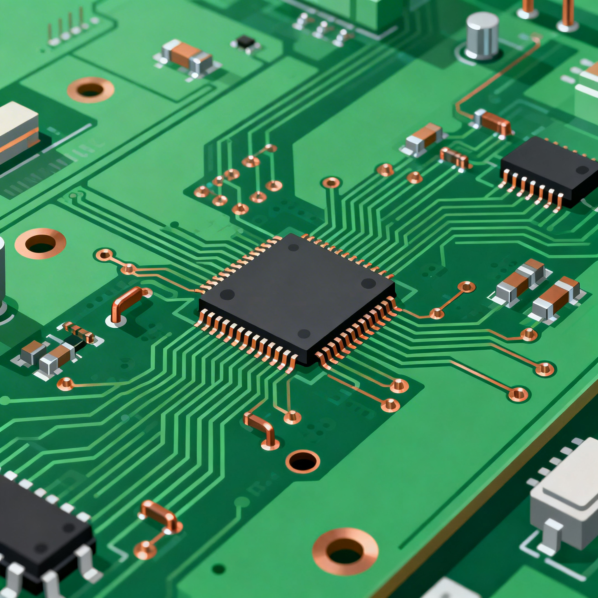
The core of PCB design involves several key elements: layout rules, stackup design, and material selection. Layout rules dictate the physical dimensions and spacing of components on the PCB, which are crucial for ensuring signal integrity and preventing electrical interference. Stackup design refers to the arrangement of conductive and insulating layers in a PCB, which affects the board's electrical performance and mechanical strength. Signal integrity is a critical factor, especially in high-speed circuits, where the integrity of signals can be compromised by crosstalk, reflections, and electromagnetic interference (EMI). Lastly, manufacturing considerations such as material properties and fabrication techniques play a vital role in determining the final quality and performance of the PCB. Understanding these technical aspects is essential for selecting the right PCB prototype supplier that aligns with specific project requirements.
Detailed Specifications
PCB design specifications are critical as they form the foundation upon which all subsequent design and manufacturing decisions are made. These specifications include trace width, spacing, via sizes, and clearances, which are fundamental to ensuring the PCB's functionality and reliability. Adherence to industry standards like IPC-2221 is crucial for achieving consistency and quality in PCB designs.
| Design Parameter | Minimum Value | Typical Value |
|---|---|---|
| Trace Width | 4 mil | 6 mil |
| Trace Spacing | 4 mil | 6 mil |
| Via Diameter | 0.2 mm | 0.3 mm |
| Annular Ring | 0.1 mm | 0.15 mm |
| Minimum Hole Size | 0.15 mm | 0.25 mm |
| Clearance to Edge | 0.5 mm | 1.0 mm |
| Board Thickness | 0.4 mm | 1.6 mm |
| Solder Mask Clearance | 0.05 mm | 0.1 mm |
| Drill to Copper | 0.2 mm | 0.3 mm |
| Aspect Ratio | 8:1 | 10:1 |
Key Takeaways from the Specifications
The specifications outlined above are crucial for maintaining the integrity and performance of a PCB. For instance, trace width and spacing are directly related to the current-carrying capacity and signal integrity of the board. Smaller trace widths might save space but could lead to overheating if not managed properly. Similarly, the aspect ratio of vias impacts the reliability of the interconnections between layers. A higher aspect ratio can lead to difficulties in plating and potential reliability issues. By adhering to these design rules, engineers can minimize risks and ensure the board performs as intended.
| Layer Configuration | Number of Layers | Application |
|---|---|---|
| Single Layer | 1 | Simple Circuits |
| Double Layer | 2 | Consumer Electronics |
| Four Layer | 4 | Telecommunications |
| Six Layer | 6 | Industrial Controls |
| Eight Layer | 8 | High-Speed Computing |
| Ten Layer | 10 | Advanced Networking |
| Twelve Layer | 12 | Aerospace Applications |
Practical Implications
The choice of layer stackup is significant in PCB design as it influences the board's electrical and mechanical performance. Single and double-layer boards are typically used for simpler applications due to their cost-effectiveness and ease of manufacturing. However, as the complexity of the application increases, additional layers are required to accommodate more intricate routing and power planes. For example, high-speed computing and advanced networking applications often necessitate eight to twelve layers to manage signal integrity and reduce crosstalk. Selecting the appropriate layer configuration is crucial for balancing performance requirements with manufacturing costs.
| Material Type | Dielectric Constant (Dk) | Loss Tangent (Df) |
|---|---|---|
| FR-4 | 4.5 | 0.02 |
| Rogers RO4350B | 3.48 | 0.0037 |
| Rogers RO3003 | 3.0 | 0.0013 |
| Nelco N4000-13 | 3.9 | 0.009 |
| Isola FR408HR | 3.75 | 0.008 |
| DuPont Pyralux | 3.4 | 0.005 |
| Megtron 6 | 3.6 | 0.002 |
| Arlon 85N | 3.5 | 0.004 |
| Panasonic R-5775(N) | 3.7 | 0.003 |
Application Guidelines
The choice of material for a PCB is pivotal in determining the board's electrical performance and suitability for specific applications. FR-4 is a popular choice for general-purpose applications due to its balanced properties and cost-effectiveness. However, for high-frequency applications, materials like Rogers RO4350B and RO3003 are preferred due to their lower dielectric constant and loss tangent, which help maintain signal integrity. Understanding these material properties allows engineers to make informed decisions that align with the performance requirements of their projects, ensuring reliability and efficiency.
Design Considerations
When designing a PCB, several considerations must be taken into account to ensure optimal performance and manufacturability. First, signal integrity should be prioritized, especially for high-speed applications, to minimize issues like crosstalk and EMI. Proper trace routing and impedance matching are essential techniques to address these challenges. Additionally, thermal management should not be overlooked; incorporating thermal vias and heat sinks can help dissipate heat effectively. Design for manufacturability (DFM) is another critical aspect, as it ensures the design can be produced efficiently and cost-effectively. This includes adhering to standard design rules and considering the capabilities of the chosen manufacturing facility. Finally, thorough testing and validation are essential to identify and address any potential issues before mass production.
Step-by-Step Implementation
1. **Define Requirements**: Begin by clearly defining the requirements of the project, including electrical, mechanical, and environmental specifications. 2. **Select Materials**: Choose suitable materials based on the application's performance and cost requirements. Consider factors like dielectric constant and thermal properties. 3. **Design Layout**: Create the PCB layout, ensuring adherence to design rules and standards. Focus on optimizing trace routing for signal integrity. 4. **Simulate Design**: Use simulation tools to validate the design, checking for potential issues like signal integrity problems and thermal hotspots. 5. **Review and Optimize**: Conduct a design review to identify areas for improvement. Optimize the design for manufacturability and cost-effectiveness. 6. **Prototype Fabrication**: Send the design to a reliable PCB prototype supplier for fabrication. Ensure they meet your quality and turnaround requirements. 7. **Testing and Validation**: Test the prototype thoroughly to ensure it meets all specifications. Conduct functional, electrical, and mechanical tests. 8. **Finalize Design**: Incorporate any necessary changes based on testing feedback and finalize the design for production.
Common Issues & Solutions
1. **Signal Integrity Problems**: Use proper trace routing and impedance control to mitigate issues like reflections and crosstalk. 2. **Thermal Management**: Implement thermal vias and heat sinks to manage heat dissipation effectively. 3. **Manufacturing Defects**: Work closely with manufacturers to ensure DFM principles are followed, reducing the risk of defects. 4. **Component Placement**: Optimize component placement to minimize trace lengths and improve signal integrity. 5. **Power Distribution**: Ensure a robust power distribution network with adequate decoupling capacitors to maintain stable voltage levels. 6. **Testing Failures**: Develop comprehensive testing protocols to identify and rectify any functional discrepancies early in the process.
Applications & Use Cases
PCBs are integral to a wide range of applications across various industries. In consumer electronics, they form the basis of devices like smartphones and tablets. In the automotive sector, PCBs are used in control systems and infotainment units. Industrial applications include automation systems and power control units. Additionally, PCBs are vital in telecommunications, supporting infrastructure like routers and switches. In the medical field, they are used in diagnostic and monitoring equipment. Each application has specific requirements that influence the choice of materials, design, and manufacturing processes.
Selection & Sourcing Guide
When selecting a PCB prototype supplier, consider factors like quality, turnaround time, and cost-effectiveness. Evaluate their adherence to industry standards such as IPC, and review their manufacturing capabilities. It's also beneficial to assess their customer support and flexibility in accommodating custom requirements. For further sourcing information, visit IC Online for a comprehensive list of suppliers and resources.
FAQ
1. **What is the importance of trace width in PCB design?** Trace width determines the current-carrying capacity and impacts signal integrity. 2. **How do I choose the right PCB material?** Consider the application's frequency, thermal requirements, and cost constraints. 3. **What are the benefits of using a multi-layer PCB?** Multi-layer PCBs offer improved signal integrity and reduced electromagnetic interference. 4. **How can I ensure my PCB design is manufacturable?** Follow DFM guidelines and collaborate with your manufacturer to align on capabilities. 5. **What is the role of a solder mask in PCB manufacturing?** A solder mask protects the PCB from oxidation and prevents solder bridging. 6. **How does layer stackup affect PCB performance?** It influences electrical performance, mechanical strength, and signal integrity. 7. **What testing is essential for PCB prototypes?** Conduct functional, electrical, and mechanical testing to validate performance. 8. **How can I manage thermal issues in my PCB design?** Use thermal vias, heat sinks, and proper layout techniques to dissipate heat. 9. **Why is signal integrity crucial in high-speed designs?** It ensures the accurate transmission of signals without distortion or loss. 10. **What is the significance of IPC standards in PCB manufacturing?** IPC standards ensure consistency, quality, and reliability in PCB designs and assemblies.
Conclusion
Selecting the right PCB prototype supplier is crucial to achieving a balance between quality, cost, and turnaround time. By understanding the intricacies of PCB design, including layout rules, stackup options, and material properties, engineers can make informed decisions that align with project requirements. Adhering to industry standards and focusing on design for manufacturability will ensure the production of reliable and efficient PCBs, ultimately contributing to the success of electronic devices across various applications.