Top PCB Prototype Suppliers: A 2026 Resource Guide for Rapid Development
Top PCB Prototype Suppliers: A 2026 Resource Guide for Rapid Development Introduction The rapid advancement of electronics technology has led to an increased demand for quick and efficient development...
Introduction
The rapid advancement of electronics technology has led to an increased demand for quick and efficient development cycles. Central to this process is the printed circuit board (PCB), which serves as the backbone of electronic devices. As we approach 2026, the importance of selecting the right PCB prototype supplier cannot be overstated. This guide aims to provide a comprehensive overview of top suppliers and the critical considerations in PCB design, layout, and manufacturing. Understanding these elements is crucial for engineers and designers striving for superior product performance and reduced time-to-market.
Technical Overview
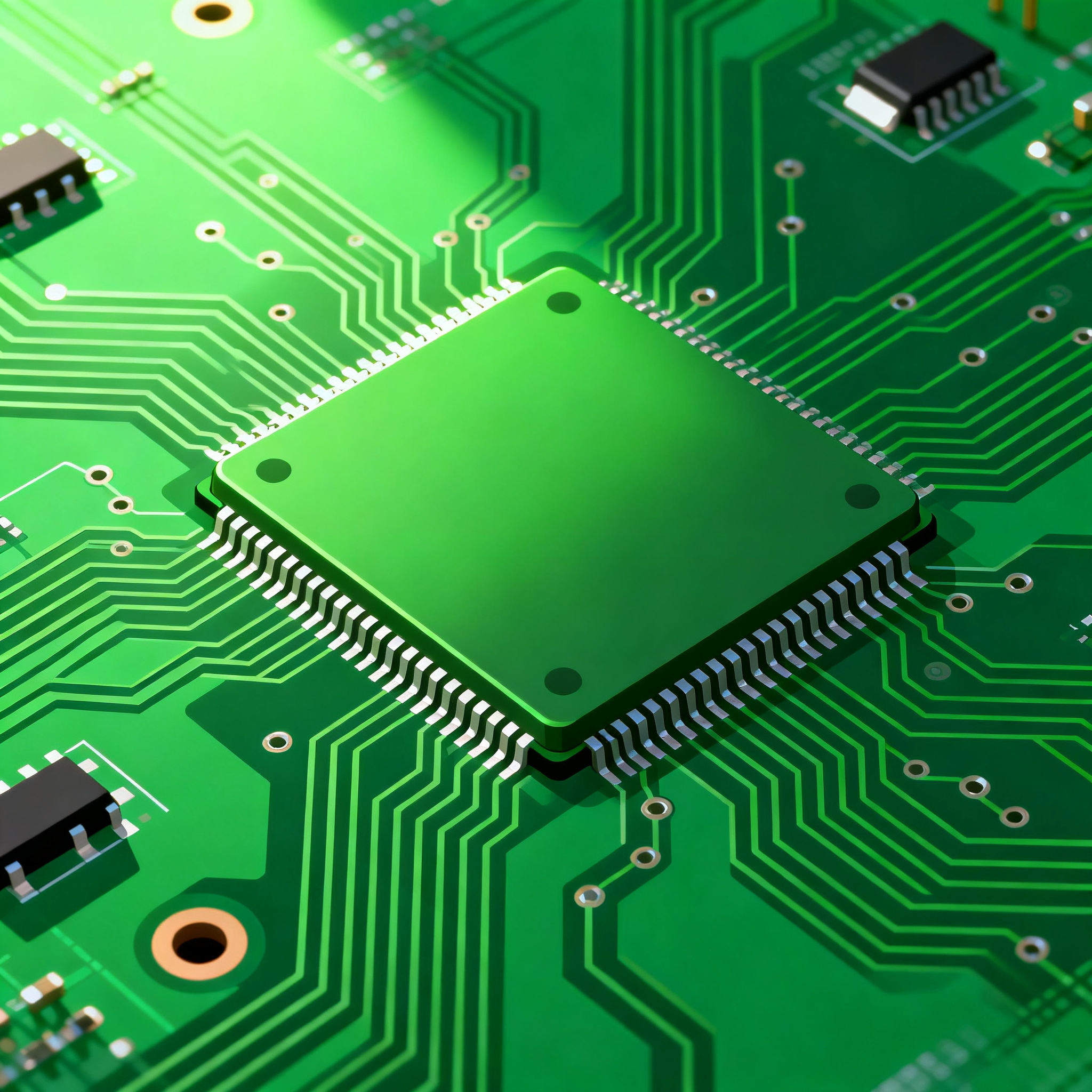
PCBs are integral to modern electronics, providing mechanical support and electrical connectivity to components. The architecture of a PCB involves multiple layers of copper and insulating material, which are etched to create pathways for electrical signals. Core concepts such as trace width, spacing, and via sizes are critical in ensuring signal integrity and manufacturability. Additionally, the stackup design significantly influences the electrical performance and thermal management of the PCB. Adhering to industry standards, like those from the IPC, ensures reliability and quality. The choice of materials, such as FR-4 or Rogers, impacts dielectric properties and loss tangent, affecting performance at high frequencies.
Detailed Specifications
Understanding the design rules and specifications of PCBs is essential for creating a reliable and efficient board. These specifications include trace width, spacing, via sizes, and clearances. Each of these parameters plays a crucial role in maintaining signal integrity and ensuring manufacturability. The following table provides a detailed overview of essential PCB design rules.
| Parameter | Minimum Value | Recommended Value |
|---|---|---|
| Trace Width | 0.1 mm | 0.2 mm |
| Trace Spacing | 0.1 mm | 0.15 mm |
| Via Size | 0.2 mm | 0.3 mm |
| Pad Diameter | 0.4 mm | 0.5 mm |
| Annular Ring | 0.05 mm | 0.1 mm |
| Clearance | 0.1 mm | 0.2 mm |
| Aspect Ratio | 6:1 | 8:1 |
| Drill Size | 0.2 mm | 0.3 mm |
| Board Thickness | 0.5 mm | 1.0 mm |
| Surface Finish | HASL | ENIG |
Key Takeaways from the Specifications
The specifications outlined in the table above are critical for ensuring the manufacturability and performance of a PCB. Trace width and spacing are particularly important for preventing crosstalk and maintaining signal integrity. The via size and pad diameter must be carefully selected to accommodate component leads and ensure reliable connections. Clearances and annular rings are essential for preventing short circuits and ensuring proper insulation between conductive elements. Engineers must balance these parameters to optimize both electrical performance and cost-effectiveness during manufacturing.
| Layer Configuration | Description | Applications |
|---|---|---|
| 2-Layer | Basic configuration with two conductive layers | Simple circuits |
| 4-Layer | Two internal layers for power and ground planes | Moderate complexity |
| 6-Layer | Four signal layers with power and ground planes | High-speed applications |
| 8-Layer | Multiple signal and ground layers for improved performance | Advanced circuits |
| 10-Layer | Optimized for high-frequency design with controlled impedance | RF applications |
| 12-Layer | Complex designs requiring extensive interconnects | Telecom and networking |
Practical Implications
The choice of layer stackup is a critical consideration in PCB design. Each configuration offers unique advantages and is suited to specific applications. For instance, a 2-layer board is cost-effective for simple designs, while an 8-layer board provides enhanced signal integrity for high-speed circuits. The additional layers in a 10 or 12-layer stackup allow for controlled impedance and are ideal for RF applications. Selecting the appropriate stackup ensures optimal performance, minimizes electromagnetic interference, and supports the necessary electrical characteristics for the application.
| Material | Dielectric Constant (Dk) | Loss Tangent |
|---|---|---|
| FR-4 | 4.5 | 0.020 |
| Rogers 4350B | 3.48 | 0.0037 |
| Rogers 4003C | 3.55 | 0.0027 |
| Isola 370HR | 4.04 | 0.019 |
| Nelco N4000-13 | 3.7 | 0.016 |
| Polyimide | 3.5 | 0.004 |
| PTFE (Teflon) | 2.1 | 0.001 |
| CEM-1 | 4.5 | 0.035 |
| Arlon 85N | 3.5 | 0.004 |
Application Guidelines
The choice of PCB material significantly influences the board's electrical performance, particularly in high-frequency applications. Materials like FR-4 are commonly used due to their cost-effectiveness and adequate performance for general applications. However, for RF and microwave applications, materials such as Rogers and PTFE offer lower dielectric constants and loss tangents, which are crucial for minimizing signal loss and maintaining integrity. Selecting the right material requires balancing performance requirements with cost considerations, ensuring the board meets the application's demands.
Design Considerations
When designing a PCB, several key considerations must be taken into account to ensure a successful outcome. Firstly, signal integrity is paramount, requiring careful attention to trace layout and impedance matching. High-speed designs benefit from controlled impedance, which can be achieved through proper stackup configuration and material choice. Thermal management is another critical factor, as heat dissipation can affect performance and reliability. Employing thermal vias and appropriate copper weight can mitigate thermal issues. Lastly, manufacturability should be considered, ensuring that the design adheres to standard manufacturing capabilities and tolerances. Collaborating closely with your PCB supplier can provide insights into optimizing the design for production.
Step-by-Step Implementation
- Define the PCB requirements: Identify the electrical, mechanical, and thermal requirements for the board.
- Select the appropriate materials: Choose materials that meet the dielectric and thermal performance needs of the application.
- Design the schematic: Create a detailed schematic capturing all components and their interconnections.
- Layout the PCB: Place components and route traces, considering signal integrity and manufacturability.
- Perform electrical simulations: Use simulation tools to verify signal integrity and identify potential issues.
- Generate manufacturing files: Create Gerber files, drill files, and a bill of materials for production.
- Prototype and test: Fabricate a prototype and conduct thorough testing to validate performance.
- Iterate and finalize: Refine the design based on test results and prepare for full-scale production.
Common Issues & Solutions
- Signal Integrity Problems: Use controlled impedance traces and maintain proper spacing to prevent crosstalk.
- Thermal Management: Integrate thermal vias and select materials with good thermal conductivity.
- Manufacturability Issues: Collaborate with suppliers to ensure design rules align with manufacturing capabilities.
- Component Placement: Optimize placement to minimize trace length and improve EMC performance.
- Power Distribution: Use wide traces and multiple ground planes to ensure stable power delivery.
- Test Point Accessibility: Design with test points for easier debugging and testing during prototyping.
Applications & Use Cases
PCBs are used across a wide range of applications, from consumer electronics to industrial systems. In telecommunications, multi-layer boards are essential for routing high-speed signals with minimal interference. In the automotive sector, PCBs must withstand harsh environments, requiring robust materials and design. Medical devices demand high reliability and precision, often utilizing advanced materials like Rogers for optimal performance. Understanding the specific requirements of each application helps guide material selection and design decisions, ensuring the final product meets performance and reliability standards.
Selection & Sourcing Guide
When selecting a PCB supplier, consider factors such as manufacturing capabilities, lead times, and quality standards. Suppliers like PCBWay and Nova PCBA offer a range of services, from prototyping to full production. It's also essential to verify the supplier's compliance with industry standards like IPC. For sourcing components, visit IC Online for a comprehensive selection of electronic components and resources.
FAQ
- What is the importance of trace width in PCB design? Trace width affects current-carrying capacity and signal integrity. Wider traces can carry more current and reduce resistive losses.
- How do I choose the right PCB material? Consider the application's frequency, thermal requirements, and cost. Materials like FR-4 are versatile, while Rogers is ideal for high-frequency designs.
- What is controlled impedance? Controlled impedance ensures consistent electrical performance across high-speed traces by maintaining a specific impedance value.
- Why are thermal vias important? Thermal vias help dissipate heat from components, improving reliability and performance by preventing overheating.
- What are the benefits of a multi-layer PCB? Multi-layer PCBs provide better signal integrity, reduced electromagnetic interference, and support for complex routing.
- How can I improve manufacturability? Adhere to standard design rules, use standard component sizes, and collaborate with your supplier to optimize the design for production.
- What is the role of a ground plane? A ground plane reduces electromagnetic interference and provides a stable reference for signals, improving overall circuit performance.
- How do I ensure signal integrity in high-speed designs? Use controlled impedance, minimize trace lengths, and maintain proper spacing between traces to reduce crosstalk.
Conclusion
In conclusion, selecting the right PCB prototype supplier and understanding the critical aspects of PCB design are essential for successful product development. By adhering to design rules, choosing appropriate materials, and optimizing layer stackups, engineers can ensure reliable and high-performance PCBs. As the industry evolves, staying informed about the latest technologies and standards will be vital for maintaining a competitive edge in the rapidly advancing electronics market.