Top 5 PCBA Manufacturing Defects and How to Prevent Costly Errors
Top 5 PCBA Manufacturing Defects and How to Prevent Costly Errors Introduction In the rapidly evolving electronics industry, Printed Circuit Board Assemblies (PCBA) play a critical role in the functio...
Introduction
In the rapidly evolving electronics industry, Printed Circuit Board Assemblies (PCBA) play a critical role in the functionality of modern devices. As electronic gadgets become more sophisticated, the demand for high-quality, defect-free PCBAs increases. This article delves into the top five manufacturing defects in PCBA and provides insights into preventing costly errors. By adhering to industry standards and best practices, manufacturers can ensure the reliability and performance of their products, thereby maintaining competitive advantage in the market.
Technical Overview
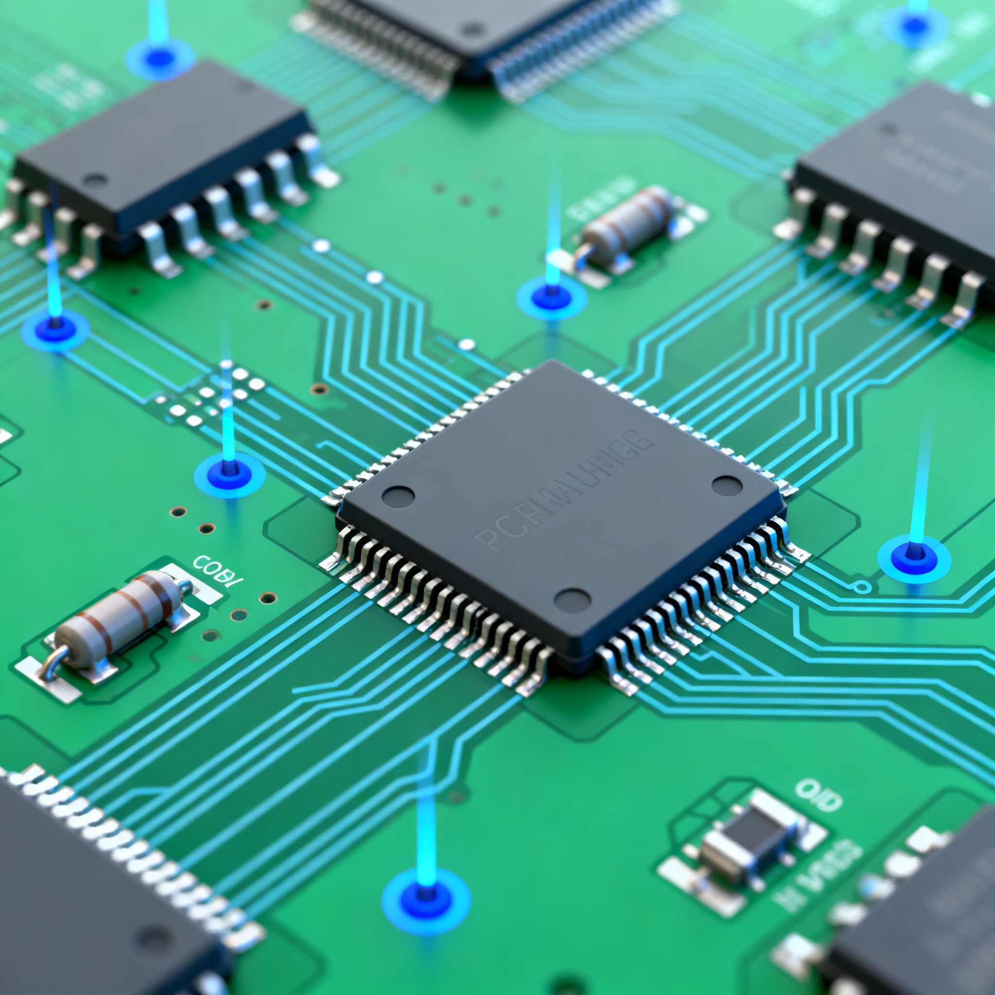
PCBA manufacturing is a complex process that involves multiple stages, from design to assembly. The core concepts of this process include PCB layout rules, stackup design, signal integrity, and manufacturing considerations. Each of these elements plays a pivotal role in ensuring the final product meets the required specifications and functions as intended. Understanding the principles behind these concepts is essential for anyone involved in the design and manufacturing of PCBAs.
PCB layout rules dictate the physical arrangement of components and traces on the board, impacting signal integrity and thermal management. Stackup design refers to the arrangement of multiple layers in a PCB, which affects electromagnetic compatibility and mechanical stability. Signal integrity encompasses the preservation of signal quality throughout the board, ensuring minimal distortion and noise. Finally, manufacturing considerations involve selecting appropriate materials and processes to meet design requirements while optimizing cost and efficiency.
Detailed Specifications
Specifications are vital in PCBA manufacturing as they define the parameters within which the board must be designed and produced. These include trace width, spacing, via sizes, and clearances, which directly affect the board's electrical performance and manufacturability. Adhering to these specifications helps to minimize defects and ensure reliable operation.
| Design Rule | Minimum Value | Notes |
|---|---|---|
| Trace Width | 4 mils | Dependent on current carrying capacity |
| Trace Spacing | 4 mils | Ensures proper isolation |
| Via Diameter | 10 mils | Standard via size for most applications |
| Annular Ring | 2 mils | Ensures reliable connections |
| Pad Size | 20 mils | Supports component mounting |
| Clearance to Edge | 10 mils | Prevents shorts and damage |
| Silkscreen Clearance | 6 mils | Ensures readability |
| Solder Mask Clearance | 4 mils | Prevents solder bridging |
| Aspect Ratio | 8:1 | Via depth to diameter ratio |
| Drill Size | 8 mils | Minimum mechanical drill size |
Key Takeaways from the Specifications
The specifications outlined in the table are critical for ensuring the manufacturability and performance of PCBAs. Trace width and spacing are particularly crucial as they affect the board's ability to handle current and prevent electrical interference. Via sizes and annular rings play a significant role in maintaining electrical connectivity and mechanical stability. By adhering to these specifications, designers can minimize the risk of defects such as shorts, opens, and thermal issues, ultimately leading to more reliable and efficient PCBAs.
| Layer Configuration | Number of Layers | Applications |
|---|---|---|
| Single Layer | 1 | Simple circuits, low-cost applications |
| Double Layer | 2 | Consumer electronics, moderate complexity |
| Four Layer | 4 | High-speed signals, EMI reduction |
| Six Layer | 6 | Complex circuits, improved signal integrity |
| Eight Layer | 8 | Advanced applications, RF circuits |
| Ten Layer | 10 | High-density interconnects, aerospace |
| Twelve Layer | 12 | High-performance computing, telecom |
Practical Implications
The choice of layer stackup configuration has significant implications on the PCB's performance and cost. Single and double layer boards are suitable for simple, low-cost applications, while multi-layer boards are essential for more complex designs requiring enhanced signal integrity and electromagnetic interference (EMI) reduction. As the number of layers increases, so does the board's ability to support high-speed signals and complex routing. However, this also raises manufacturing costs. Designers must balance performance requirements with budget constraints when selecting a stackup configuration.
| Material | Dielectric Constant (Dk) | Loss Tangent (Df) |
|---|---|---|
| FR-4 | 4.5 | 0.020 |
| Rogers 4350B | 3.66 | 0.0037 |
| Rogers RO3003 | 3.00 | 0.0013 |
| Isola 370HR | 4.04 | 0.019 |
| Nelco N4000-13 | 3.90 | 0.016 |
| Panasonic Megtron 6 | 3.5 | 0.002 |
| Arlon 85N | 3.5 | 0.004 |
| DuPont Pyralux | 3.4 | 0.002 |
| Rogers RO4350 | 3.48 | 0.0031 |
Application Guidelines
The choice of material for a PCB is crucial as it affects the board's electrical performance and thermal management. FR-4 is the most commonly used material due to its balance of cost and performance. However, for high-frequency applications, materials like Rogers 4350B and RO3003 are preferred due to their lower dielectric constant and loss tangent, which reduce signal loss and improve signal integrity. Understanding the properties of each material allows designers to select the most appropriate option for their specific application, ensuring optimal performance and reliability.
Design Considerations
When designing a PCB, several considerations must be taken into account to ensure a successful outcome. These include adhering to design rules, selecting the appropriate stackup configuration, and choosing the right materials. Additionally, designers must consider signal integrity, thermal management, and manufacturability.
Signal integrity is paramount in ensuring that signals are transmitted with minimal distortion and noise. This involves careful routing of traces, proper grounding, and the use of differential pairs where necessary. Thermal management is also critical, as excessive heat can lead to component failure and reduced reliability. This can be addressed through the use of thermal vias, heat sinks, and careful component placement.
Manufacturability is another key consideration. Designers must work closely with manufacturers to ensure that the design can be produced efficiently and cost-effectively. This involves understanding the capabilities and limitations of the manufacturing process and making design decisions accordingly.
Step-by-Step Implementation
- Define the project requirements and constraints, including electrical performance, mechanical size, and budget.
- Select the appropriate materials based on the application's frequency, thermal requirements, and cost considerations.
- Determine the optimal layer stackup configuration to balance performance and cost.
- Adhere to design rules, including trace width, spacing, via sizes, and clearances, to ensure manufacturability and performance.
- Perform signal integrity analysis to identify potential issues such as crosstalk, reflection, and EMI.
- Address thermal management through the use of thermal vias, heat sinks, and strategic component placement.
- Collaborate with the manufacturing team to ensure the design is compatible with their capabilities and processes.
- Conduct thorough testing and validation to verify the design meets all specifications and requirements.
Common Issues & Solutions
Despite best efforts, manufacturing defects can still occur. Here are some common issues and their solutions:
- Short Circuits: Caused by solder bridging or inadequate trace spacing. Prevent by adhering to spacing rules and using solder mask.
- Open Circuits: Result from incomplete solder joints or broken traces. Ensure proper soldering techniques and inspect for defects.
- Component Misalignment: Occurs during assembly. Use precise pick-and-place machines and alignment marks.
- Thermal Issues: Overheating can damage components. Implement effective thermal management strategies.
- Signal Integrity Problems: Caused by poor routing or impedance mismatches. Conduct signal integrity analysis and optimize routing.
Applications & Use Cases
PCBAs are used in a wide range of applications, from consumer electronics to aerospace. In consumer electronics, they are found in smartphones, tablets, and wearable devices, where compact size and high performance are critical. In the automotive industry, PCBAs are used in engine control units, infotainment systems, and advanced driver-assistance systems (ADAS). In aerospace, they are used in avionics systems, where reliability and performance are paramount. Each application has unique requirements, and the design and manufacturing process must be tailored accordingly.
Selection & Sourcing Guide
When selecting and sourcing components for a PCBA project, it is essential to consider factors such as availability, cost, and compatibility with the design. IC Online is a valuable resource for sourcing electronic components, offering a wide range of products from leading manufacturers.
FAQ
- What is the importance of trace width in PCB design? Trace width affects the board's current carrying capacity and resistance. It is critical for ensuring reliable electrical performance.
- How does layer stackup affect PCB performance? The stackup configuration impacts signal integrity, EMI, and mechanical stability. It is essential for high-speed and complex designs.
- Why is signal integrity analysis important? Signal integrity analysis helps identify potential issues such as crosstalk and reflection, ensuring the board functions as intended.
- What materials are best for high-frequency applications? Materials like Rogers 4350B and RO3003 are preferred for high-frequency applications due to their low dielectric constant and loss tangent.
- How can thermal issues be addressed in PCB design? Thermal issues can be addressed through the use of thermal vias, heat sinks, and strategic component placement.
- What are common causes of open circuits in PCBAs? Open circuits can be caused by incomplete solder joints or broken traces. Proper soldering techniques and inspection are essential.
- How does solder mask prevent short circuits? Solder mask provides an insulating layer between traces, preventing solder bridging and short circuits.
- What is the role of via sizes in PCB design? Via sizes impact the board's electrical connectivity and mechanical stability. They must be carefully selected to meet design requirements.
- How can component misalignment be prevented during assembly? Component misalignment can be prevented by using precise pick-and-place machines and alignment marks.
- What are the benefits of using multi-layer PCBs? Multi-layer PCBs offer enhanced signal integrity, EMI reduction, and support for complex routing, making them ideal for advanced applications.
Conclusion
In conclusion, understanding and addressing the top PCBA manufacturing defects is crucial for ensuring high-quality, reliable products. By adhering to industry standards and best practices, designers and manufacturers can minimize defects, optimize performance, and reduce costs. This comprehensive guide provides valuable insights into PCB design rules, stackup options, material properties, and practical considerations, empowering professionals to make informed decisions and achieve success in their projects.