Top 5 PCBA Manufacturing Defects and How to Avoid Them in Your Production Line
Top 5 PCBA Manufacturing Defects and How to Avoid Them in Your Production Line Introduction In the rapidly evolving world of electronics, Printed Circuit Board Assemblies (PCBA) form the backbone of m...
Introduction
In the rapidly evolving world of electronics, Printed Circuit Board Assemblies (PCBA) form the backbone of most electronic devices. The integrity and functionality of these assemblies are pivotal to the performance and reliability of the final product. Understanding common manufacturing defects and how to avoid them is crucial for any engineer involved in PCB design and production. This article explores the top five PCBA manufacturing defects and provides guidance on preventing them through meticulous design and manufacturing practices.
Technical Overview
The core of PCBA manufacturing involves several intricate processes, from designing the PCB layout to assembling components. Key elements such as PCB layout rules, stackup design, signal integrity, and manufacturing considerations play a significant role in ensuring a defect-free product. Adhering to standards like IPC-A-610 and IPC-2221 is essential for maintaining quality and consistency. Moreover, understanding the principles of signal integrity and electromagnetic compatibility helps in minimizing defects related to interference and noise.
- PCB Layout Rules: Ensuring proper trace width, spacing, and via sizes is crucial to prevent issues like short circuits and signal interference.
- Layer Stackup Design: Effective stackup design helps in managing impedance and reducing crosstalk.
- Signal Integrity: Maintaining signal integrity involves minimizing noise and distortion, which can lead to malfunctioning of circuits.
- Manufacturing Considerations: Understanding the manufacturing capabilities and limitations helps in designing PCBs that are easier to produce and assemble.
Detailed Specifications
Specifications are the foundation of any successful PCB design. They guide the design process and ensure that the final product meets the required performance standards. Important specifications include trace width, spacing, via sizes, and clearances. These parameters are vital for ensuring signal integrity and preventing common manufacturing defects.
| Design Parameter | Recommended Value | Significance |
|---|---|---|
| Trace Width | 0.15 mm - 0.3 mm | Prevents overheating and maintains current capacity |
| Trace Spacing | 0.2 mm | Reduces risk of short circuits |
| Via Sizes | 0.3 mm - 0.6 mm | Ensures reliable connections between layers |
| Pad Sizes | 0.5 mm - 0.7 mm | Facilitates proper soldering of components |
| Clearance | 0.2 mm | Minimizes risk of electrical shorts |
| Aspect Ratio | 8:1 | Ensures manufacturability and reliability of vias |
| Solder Mask Clearance | 0.1 mm | Prevents solder bridging |
| Silkscreen Clearance | 0.1 mm | Maintains readability and prevents overlap with pads |
| Min Hole Size | 0.3 mm | Ensures drill accuracy and reliability |
| Board Thickness | 1.6 mm | Provides structural integrity |
Key Takeaways from the Specifications
The data in the table highlights the critical aspects of PCB design that affect manufacturing quality and performance. For instance, maintaining appropriate trace width and spacing is essential to prevent overheating and short circuits. Proper via and pad sizes ensure reliable interconnections and facilitate effective soldering. These specifications are vital in minimizing defects and ensuring high-quality PCB assemblies.
| Layer Configuration | Use Case | Benefits |
|---|---|---|
| 2-Layer | Simple designs | Cost-effective, easy to manufacture |
| 4-Layer | Moderate complexity | Improved signal integrity, reduced EMI |
| 6-Layer | Complex designs | Better power distribution, reduced crosstalk |
| 8-Layer | High-speed applications | Enhanced signal integrity, EMI control |
| 10-Layer | Advanced RF designs | Superior isolation, impedance control |
| 12-Layer | High-density interconnects | Optimal for compact designs, high performance |
Practical Implications
The layer stackup options presented here are crucial for achieving the desired performance in different applications. For example, a 4-layer configuration is ideal for moderate complexity designs, offering a balance between cost and performance. In contrast, an 8-layer stackup is suitable for high-speed applications, providing enhanced signal integrity and EMI control. Understanding these configurations helps in selecting the right stackup for specific design requirements, thereby reducing manufacturing defects and optimizing performance.
| Material | Dielectric Constant (Dk) | Loss Tangent |
|---|---|---|
| FR-4 | 4.4 | 0.02 |
| Rogers 4350B | 3.48 | 0.0037 |
| Rogers 4003C | 3.55 | 0.0027 |
| Isola FR408 | 3.68 | 0.009 |
| Arlon 85N | 3.5 | 0.004 |
| Nelco N4000-13 | 3.7 | 0.016 |
| Duroid 5880 | 2.2 | 0.0009 |
| Taconic RF-35 | 3.5 | 0.0018 |
| Megtron 6 | 3.6 | 0.003 |
| Polyclad 370HR | 3.8 | 0.015 |
Application Guidelines
Material properties such as dielectric constant and loss tangent are critical in determining the performance of PCBs, especially in high-frequency applications. For instance, Rogers 4350B is preferred for RF applications due to its low loss tangent and stable dielectric constant. On the other hand, FR-4 is a cost-effective choice for general-purpose applications. Selecting the appropriate material based on these properties ensures optimal performance and reliability of the final product.
Design Considerations
Designing a PCB involves numerous considerations to ensure functionality and manufacturability. Key aspects include:
- Thermal Management: Proper heat dissipation techniques such as thermal vias and heat sinks are essential to prevent overheating.
- Component Placement: Strategically placing components reduces trace lengths and minimizes signal interference.
- Ground and Power Planes: Implementing dedicated planes helps in reducing noise and maintaining signal integrity.
- Design for Manufacturability (DFM): Ensures that designs are compatible with manufacturing capabilities, reducing potential defects.
By adhering to these considerations, designers can create PCBs that are not only functional but also easy to manufacture and assemble, minimizing the risk of defects.
Step-by-Step Implementation
Implementing a defect-free PCBA manufacturing process involves several critical steps:
- Design Validation: Ensure the design meets all specifications and standards before proceeding to manufacturing.
- Material Selection: Choose materials that align with the performance requirements and operating conditions of the PCB.
- Prototyping: Create prototypes to test and validate the design under real-world conditions.
- DFM Analysis: Conduct a thorough design for manufacturability analysis to identify potential issues before production.
- Supplier Collaboration: Work closely with suppliers to understand manufacturing capabilities and limitations.
- Quality Control: Implement rigorous quality control measures throughout the manufacturing process to detect and rectify defects early.
- Continuous Improvement: Gather feedback from production and incorporate it into future designs to enhance quality and reduce defects.
- Documentation: Maintain comprehensive documentation of the design and manufacturing process for future reference and troubleshooting.
Following these steps ensures a streamlined process, reducing the likelihood of defects and improving the overall quality of the PCBA.
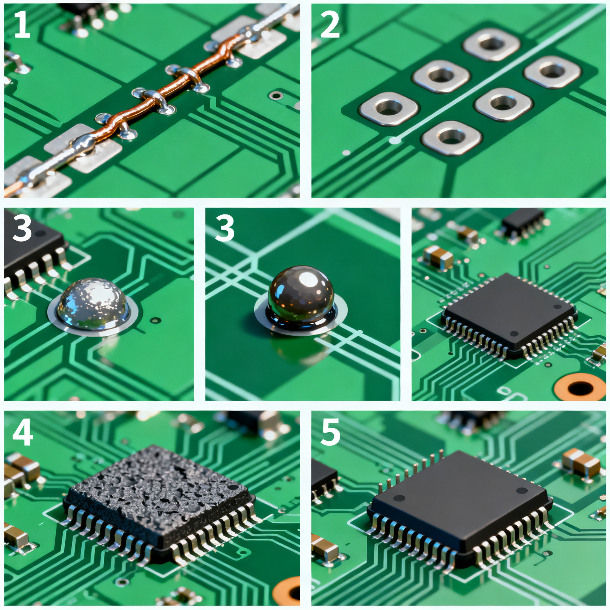
Common Issues & Solutions
Despite best efforts, certain issues can still arise during PCBA manufacturing. Here are some common problems and their solutions:
- Insufficient Solder Joint: Ensure proper stencil design and solder paste application to achieve reliable solder joints.
- Component Misalignment: Use automated pick-and-place machines and verify alignment with optical inspection systems.
- Delamination: Select materials with appropriate thermal properties and avoid excessive heating during reflow.
- Electromagnetic Interference (EMI): Implement proper shielding and grounding techniques to minimize EMI.
- Open Circuits: Conduct thorough electrical testing to identify and rectify open circuits before final assembly.
- Short Circuits: Maintain adequate spacing between traces and components to prevent accidental shorts.
Addressing these issues proactively helps in maintaining high-quality standards and reducing production costs.
Applications & Use Cases
PCBA is utilized in a wide range of applications, from consumer electronics to industrial machinery. Some real-world examples include:
- Consumer Electronics: Smartphones, tablets, and laptops rely heavily on PCBAs for compact and efficient design.
- Automotive Industry: Advanced driver-assistance systems (ADAS) and infotainment systems use PCBAs for enhanced functionality.
- Medical Devices: Reliable and precise PCBAs are critical in medical diagnostics and monitoring equipment.
- Aerospace: High-reliability PCBAs are essential for avionics and satellite systems.
These applications demonstrate the versatility and importance of PCBA in modern technology.
Selection & Sourcing Guide
When selecting and sourcing components for PCBA, it's important to consider:
- Supplier Reliability: Choose reputable suppliers with a track record of quality and timely delivery.
- Component Specifications: Ensure components meet the required specifications and standards for your application.
- Cost Considerations: Balance cost with performance to achieve optimal value.
For more information on sourcing components, visit IC Online.
FAQ
- What is the most common defect in PCBA manufacturing? Solder joint defects are among the most common, often caused by improper solder paste application or reflow profiles.
- How can I improve signal integrity in my PCB design? Utilize proper layer stackup, maintain adequate trace spacing, and implement ground planes to improve signal integrity.
- What role does the dielectric constant play in PCB design? The dielectric constant affects the signal speed and impedance, influencing the overall performance of the PCB.
- How do I select the right PCB material for my application? Consider factors such as frequency, thermal requirements, and mechanical properties when selecting PCB materials.
- What is the significance of IPC standards in PCB manufacturing? IPC standards provide guidelines for design, assembly, and quality assurance, ensuring consistency and reliability in PCB manufacturing.
- How can I prevent component misalignment during assembly? Use automated placement machines and conduct optical inspections to ensure precise component alignment.
- What are the benefits of using a multi-layer PCB stackup? Multi-layer stackups offer improved signal integrity, reduced EMI, and better power distribution, enhancing overall performance.
- How do I ensure manufacturability in my PCB design? Conduct a design for manufacturability (DFM) analysis to identify potential issues and ensure compatibility with manufacturing processes.
- What is the impact of loss tangent on PCB performance? A lower loss tangent indicates less signal loss, which is crucial for high-frequency applications to maintain signal integrity.
- How can I reduce electromagnetic interference (EMI) in my PCBA? Implement proper grounding, shielding, and trace routing techniques to minimize EMI in your PCBA design.
Conclusion
Ensuring a defect-free PCBA manufacturing process requires a thorough understanding of design specifications, material properties, and manufacturing techniques. By adhering to industry standards and implementing best practices, engineers can significantly reduce defects and enhance the quality and reliability of PCBAs. This comprehensive guide provides valuable insights and practical steps to achieve excellence in PCBA manufacturing.