Thermal Management in PCBs: Effective Strategies for Heat Dissipation in Multi-Layer Boards
Thermal Management in PCBs: Effective Strategies for Heat Dissipation in Multi-Layer Boards table { border: 1px solid #000; border-collapse: collapse; width: 100%; margin: 20px 0; } th, td { border: 1...
Introduction
In the rapidly evolving electronics industry, thermal management has become a critical aspect of printed circuit board (PCB) design, especially in multi-layer boards. With the increasing complexity and miniaturization of electronic components, effective heat dissipation is essential to ensure reliability and performance. This article explores various strategies for thermal management in PCBs, focusing on design rules, stackup configurations, signal integrity, and manufacturing considerations.
Technical Overview
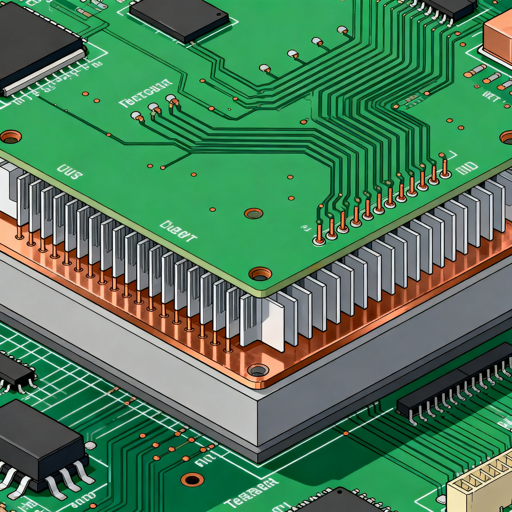
Thermal management in PCBs involves the strategic design of board layouts to efficiently dissipate heat generated by electronic components. The core principles include optimizing trace widths, via sizes, and clearances to facilitate heat flow, as well as selecting appropriate materials with favorable thermal properties. Multi-layer boards present unique challenges due to their complex architecture, which requires careful consideration of layer stackups to balance thermal performance with electrical functionality and manufacturability.
Detailed Specifications
When designing PCBs for optimal thermal management, several specifications must be considered. These include trace width and spacing, via sizes, and clearances. Each of these factors plays a critical role in the board's ability to dissipate heat effectively. The following table outlines standard design rules that can be applied to enhance thermal performance in multi-layer PCBs.
| Parameter | Standard Value | Comments |
|---|---|---|
| Trace Width | 0.15 mm | Standard for signal traces, wider for power traces |
| Trace Spacing | 0.20 mm | Minimum to prevent crosstalk |
| Via Diameter | 0.30 mm | Standard for signal vias, larger for thermal vias |
| Via Pad Diameter | 0.60 mm | Ensures reliable connection |
| Clearance to Edge | 0.50 mm | Prevents electrical shorts |
| Thermal Relief Pad | 0.80 mm | Improves solderability |
| Power Plane Clearance | 0.25 mm | Reduces risk of shorts |
| Ground Plane Clearance | 0.25 mm | Maintains signal integrity |
| Solder Mask Clearance | 0.10 mm | Ensures proper coverage |
| Silkscreen Clearance | 0.15 mm | Avoids overlapping with pads |
Key Takeaways from the Specifications
The specifications outlined in the table are critical for ensuring effective thermal management in multi-layer PCBs. Trace width and spacing are particularly important for minimizing resistance and facilitating heat dissipation. Similarly, via sizes and clearances play a crucial role in providing thermal paths and preventing electrical shorts. By adhering to these design rules, engineers can optimize the thermal performance and reliability of their PCB designs.
| Configuration | Description | Applications |
|---|---|---|
| 2-Layer | Basic configuration with one signal and one ground layer | Simple circuits, low-power applications |
| 4-Layer | Two signal layers, one ground, one power plane | Medium complexity, improved thermal performance |
| 6-Layer | Four signal layers, one ground, one power plane | Complex designs, enhanced signal integrity |
| 8-Layer | Six signal layers, one ground, one power plane | Advanced designs, high-speed applications |
| 10-Layer | Eight signal layers, one ground, one power plane | High-density interconnects, RF applications |
| 12-Layer | Ten signal layers, one ground, one power plane | Very complex systems, maximum thermal management |
Practical Implications
The choice of layer stackup has significant implications for both thermal and electrical performance. While a 2-layer stackup is suitable for simple, low-power designs, more complex applications benefit from additional layers that provide dedicated paths for power and ground. This not only enhances thermal dissipation but also improves signal integrity. Engineers must carefully select the appropriate configuration to balance performance, cost, and manufacturability.
| Material | Dielectric Constant (εr) | Loss Tangent (tan δ) |
|---|---|---|
| FR-4 | 4.5 | 0.020 |
| Rogers 4350B | 3.66 | 0.0037 |
| Rogers 4003C | 3.55 | 0.0027 |
| Isola FR408 | 3.75 | 0.0095 |
| Nelco N4000-13 | 3.7 | 0.009 |
| Rogers TMM10i | 9.8 | 0.002 |
| Arlon 85N | 3.5 | 0.004 |
| Panasonic Megtron 6 | 3.5 | 0.003 |
| Isola I-Tera MT40 | 3.45 | 0.0031 |
| Rogers RT/duroid 5880 | 2.20 | 0.0009 |
Application Guidelines
When selecting materials for PCB construction, dielectric constant and loss tangent are crucial parameters. FR-4 is the industry standard for most applications due to its balance of cost and performance. However, for high-frequency or RF applications, materials like Rogers and Arlon with lower dielectric constants and loss tangents are preferred for their superior signal integrity and reduced signal loss. Engineers must consider these properties in conjunction with thermal requirements to select the most appropriate material for their specific application.
Design Considerations
Effective thermal management in PCB design requires a holistic approach that integrates multiple design considerations. Engineers must account for component placement, trace routing, and the use of thermal vias to facilitate heat dissipation. Additionally, the use of thermal pads and heat sinks can provide additional pathways for heat to escape from critical components. It is also important to consider the thermal conductivity of materials and the impact of environmental factors such as airflow and ambient temperature on the overall thermal performance of the board.
When designing for thermal management, engineers should:
- Optimize component placement to minimize thermal hotspots.
- Use wider traces for power and ground connections to reduce resistance.
- Incorporate thermal vias to connect internal layers and dissipate heat.
- Utilize thermal relief pads to improve solderability and heat flow.
- Select materials with appropriate thermal and electrical properties.
- Consider the use of heat sinks and thermal interface materials for high-power components.
- Ensure adequate clearance between components to allow for natural convection.
- Implement thermal simulation tools to predict and analyze heat distribution.
Step-by-Step Implementation
Implementing effective thermal management strategies in PCB design involves a series of steps that ensure optimal heat dissipation and reliability. The following steps outline the process for designing a multi-layer PCB with efficient thermal management:
- Define Design Requirements: Begin by understanding the thermal requirements of the application, including power dissipation, ambient temperature, and cooling methods.
- Select Appropriate Materials: Choose materials with suitable thermal and electrical properties based on the application's frequency and thermal load.
- Design Layer Stackup: Configure the layer stackup to balance thermal and electrical performance, ensuring dedicated power and ground planes for heat dissipation.
- Optimize Component Placement: Position components to minimize thermal hotspots and ensure even heat distribution across the board.
- Route Traces and Vias: Use wider traces for power connections and incorporate thermal vias to facilitate heat flow between layers.
- Apply Thermal Relief Pads: Implement thermal relief pads on vias and pads to improve solderability and heat transfer.
- Conduct Thermal Analysis: Use simulation tools to model heat distribution and identify potential hotspots or areas of concern.
- Finalize Design and Validation: Review and validate the design against industry standards and manufacturing capabilities to ensure compliance and manufacturability.
Common Issues & Solutions
Despite careful design, PCBs can encounter thermal management issues that impact performance and reliability. Here are some common problems and their solutions:
- Thermal Hotspots: Caused by high-power components concentrated in a small area. Solution: Distribute components evenly and use thermal vias to dissipate heat.
- Insufficient Heat Dissipation: Due to inadequate trace width or thermal vias. Solution: Increase trace width and add more thermal vias to improve heat flow.
- Poor Material Selection: Using materials with high dielectric loss or low thermal conductivity. Solution: Select materials with favorable thermal and electrical properties for the application.
- Inadequate Cooling: Lack of airflow or heat sinks. Solution: Implement active cooling methods such as fans or heat sinks to enhance heat dissipation.
- Signal Integrity Issues: Caused by improper layer stackup or material choice. Solution: Optimize layer stackup and select low-loss materials for high-frequency applications.
- Solder Joint Failures: Due to excessive heat or thermal expansion. Solution: Use thermal relief pads and appropriate soldering techniques to ensure reliable connections.
Applications & Use Cases
Thermal management is critical in a wide range of applications, from consumer electronics to industrial systems. In high-performance computing, efficient heat dissipation ensures the reliability and longevity of processors and memory modules. In automotive and aerospace applications, effective thermal management is essential to withstand harsh environmental conditions and maintain system performance. Additionally, in telecommunications, managing heat in RF and microwave circuits is crucial for maintaining signal integrity and reducing noise.
Selection & Sourcing Guide
When selecting components and materials for PCB design, it is important to consider both performance and availability. Engineers can source components from reputable suppliers such as IC Online, which offers a wide range of electronic components and materials suitable for various applications. By partnering with reliable suppliers, engineers can ensure the quality and consistency of their designs.
FAQ
- What is the importance of thermal management in PCBs? Thermal management is crucial for ensuring the reliability and performance of electronic components by preventing overheating and thermal damage.
- How can I improve heat dissipation in a multi-layer PCB? Use wider traces, thermal vias, and appropriate materials, and consider active cooling methods such as heat sinks and fans.
- What materials are best for high-frequency applications? Materials like Rogers and Arlon with low dielectric constants and loss tangents are ideal for high-frequency applications.
- How do thermal vias work? Thermal vias provide a conductive path for heat to flow from the surface layers to internal layers or heat sinks, enhancing heat dissipation.
- What is a thermal relief pad? A thermal relief pad is a design feature that improves solderability and heat transfer by connecting a via or pad to a copper plane with a web of narrow traces.
- Can I use FR-4 for RF applications? While FR-4 can be used in some RF applications, materials with lower dielectric loss like Rogers are preferred for better signal integrity.
- What are the challenges of thermal management in automotive electronics? Automotive electronics must withstand high temperatures and harsh conditions, requiring robust thermal management solutions.
- How do I perform thermal analysis on a PCB? Use simulation tools to model heat distribution and identify potential hotspots, allowing for design adjustments to improve thermal performance.
- What role do heat sinks play in thermal management? Heat sinks increase the surface area for heat dissipation, allowing for more efficient cooling of high-power components.
- How does layer stackup affect thermal management? The layer stackup determines the arrangement of power and ground planes, impacting heat dissipation and signal integrity.
Conclusion
Effective thermal management is essential for the reliability and performance of multi-layer PCBs. By understanding and implementing design rules, selecting appropriate materials, and optimizing layer stackups, engineers can enhance heat dissipation and ensure the longevity of electronic components. As technology continues to advance, the importance of thermal management will only increase, making it a critical consideration in PCB design and manufacturing.