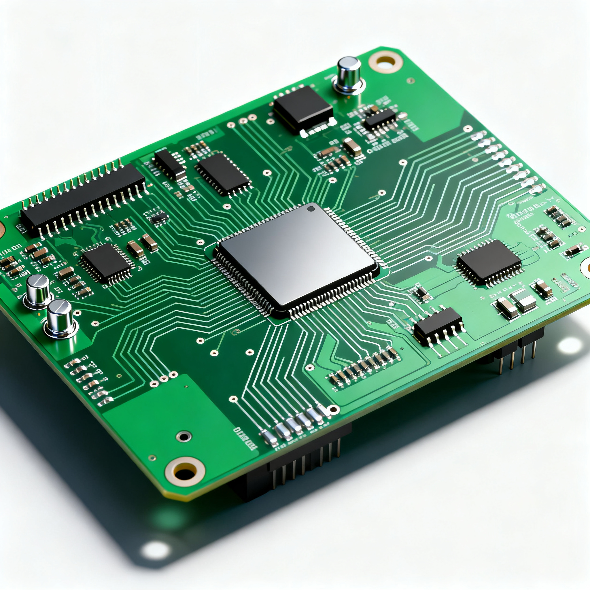
The Engineer’s Step-by-Step Guide to Using the 2025 PCBA Directory for High-Reliability, 6-Layer HDI Assemblies
When a 6-Layer HDI Assembly Failure Grounds a Product Line: The Stakes in 2025 You've seen the post-mortem photos. A hairline crack radiating from a microvia barrel, a lifted BGA pad after 800 thermal...
When a 6-Layer HDI Assembly Failure Grounds a Product Line: The Stakes in 2025
You've seen the post-mortem photos. A hairline crack radiating from a microvia barrel, a lifted BGA pad after 800 thermal cycles, or a solder joint that separated cleanly from the copper fill — each failure mode carries the same message: your 6-layer HDI assembly was never built to survive the field. When failure modes are being investigated, application of the relevant tests involve cumulatively stressing the PCBA until failure (thermal, mechanical, and environmental), followed by examining the board to locate and examine the specific failure as Zach Peterson details in Altium's reliability analysis overview. The root cause is rarely a single event. It's the accumulation of sequential lamination stresses, incomplete plasma desmear, and microvia target-land misregistration that silently degrades interconnect integrity over months of thermal cycling.
The landscape has shifted dramatically. With the explosion of AI compute modules, Low Earth Orbit (LEO) satellite communications, and L3 autonomous driving platforms, the "simple" printed circuit board has evolved into a high-performance engine. For OEMs in Europe and North America, the stakes have never been higher. A single solder joint failure or a sub-standard component can lead to catastrophic recalls as JYPCBA's analysis of high-reliability PCBA manufacturing confirms. When your 6-layer HDI assembly sits inside a vehicle's domain controller processing 50 trillion operations per second, or routes phased-array beamforming signals in a satellite that nobody can service, the margin for error collapses to zero.
Faulty assemblies don't just fail in the field — they trigger system-level failures, costly recalls, and permanently damaged reputations, especially in critical sectors like medical devices and automotive electronics HCDPCBA notes in their guide to high-reliability assembly. Regulatory bodies are watching. One public recall attributable to a PCB assembly defect can unravel years of supplier qualification work. The defense against this isn't hope — it's a methodical sourcing strategy anchored in the 2025 PCBA directory, where you can identify partners who adhere to industry standards (IPC-2221, IPC-A-610) and employ Failure Mode and Effects Analysis (FMEA) to identify vulnerabilities early per LTPCBA's reliability enhancement framework.
Key Takeaway: The directory isn't a phone book. It's a filtering tool that separates suppliers who understand the physics of failure from those who simply list "HDI" on their capability sheet. When you're sourcing a 6-layer HDI assembly that must survive 2,000+ thermal cycles in a harsh environment, the directory's certification tags, process documentation, and audit trails become your first line of defense.
How a High-Reliability 6-Layer HDI Stack-Up Defines Your Assembly's Signal and Mechanical Integrity
Before you can evaluate a supplier, you need to understand the stack-up you're asking them to build. A 6-layer HDI board isn't simply a thinner version of a standard multilayer. The interconnect architecture — the way signals travel between layers — fundamentally changes once you introduce microvias, and the choices you make here ripple through every aspect of manufacturing cost, lead time, and field reliability.
A blind via connects an outer layer to an inner layer. A buried via connects internal layers only. Via-in-pad places a via inside a component pad, often for fine-pitch BGA routing. For formal HDI design terminology and microvia guidance, engineers often refer to the IPC-2226 HDI printed board design standard as outlined in Weller PCB's comprehensive HDI sourcing guide. These definitions aren't academic — they determine whether your 0.8mm-pitch BGA can escape all its signals without adding layers, and whether your 6-layer board can survive the thermal expansion mismatches that come with dense via fields.
The manufacturing process itself introduces complexity. The manufacturer processes the core, adds dielectric and copper layers, forms vias, plates them, and repeats the process as needed. More lamination cycles usually mean more cost, longer lead time, and more chances for registration or reliability issues AllPCB explains in their step-by-step HDI manufacturing guide. Each lamination cycle exposes the partially built board to high pressure and temperature, and every subsequent laser-drilling step must align precisely with the buried features from previous cycles. A 2-mil misregistration on cycle three can put a microvia land partially off its target pad — a defect that passes electrical test at ICT but fails after 300 thermal cycles in the field.
Sequential lamination ensures reliable interconnects, which are essential for maintaining signal integrity at high frequencies. However, it also increases manufacturing time and cost due to the multiple lamination cycles, sometimes requiring 3 to 5 cycles for a single board according to AllPCB's process documentation. A 6-layer board with a 2+4+2 construction (two sequential lamination cycles building up from a 4-layer core) represents a sweet spot for many high-reliability applications, but the exact construction type matters enormously.
The IPC-2226 standard defines HDI construction types from Type 1 through Type 6, and the IPC-4104 standard helps identify materials concerning stack-up to meet dielectric performance and high-precision HDI structures as Viasion's HDI design guide details. Type 5 and Type 6 constructions — coreless and ELIC (Every Layer Interconnect) — push the boundaries of what's possible but demand the most sophisticated process control.
| Parameter | Typical 6-Layer HDI (2+4+2) | 6-Layer ELIC Construction | Impact on Reliability & Sourcing |
|---|---|---|---|
| Lamination cycles | 2–3 | 5–6 (every layer pair) | Each cycle adds registration risk; ELIC demands tighter process control |
| Microvia type | Blind (L1–L2, L5–L6), buried (L2–L5) | Stacked microvias through all layers | Stacked vias require copper filling and planarization at each stage |
| Typical min. trace/space | 75μm / 75μm (3/3 mil) | 50μm / 50μm (2/2 mil) | Finer geometries demand laser direct imaging (LDI) and tighter cleanroom control |
| Microvia aspect ratio | 0.8:1 to 1:1 | 0.6:1 to 0.8:1 | Lower AR = more reliable copper plating in microvia barrel |
| Dielectric material | FR-4 high-Tg (170°C+) or mid-loss | Low-loss (Megtron 4/6, Rogers 4350B) | Material choice affects Z-axis CTE and microvia reliability under thermal cycling |
| Via-in-pad capability | Yes, with copper fill + planarization | Standard (part of ELIC process) | Via-in-pad costs 15–25% more per board; verify fill voiding with X-ray |
| Typical lead time (bare PCB) | 10–15 working days | 18–25 working days | ELIC: budget 1.5–2× standard HDI lead time |
| Registration tolerance | ±50μm | ±35μm | Tighter tolerance = lower risk of microvia target-land breakout |
| Primary failure modes | Microvia barrel crack, pad cratering | Stacked via separation, plating void | FMEA should address both; IST testing recommended for qualification |
When you use the PCBA directory, these parameters become your screening criteria. A supplier listing "6-layer HDI — 2 lamination cycles" tells you something useful. One that simply says "HDI up to 24 layers" without specifying construction type, microvia aspect ratio capability, or material options hides critical information. The directory's search and filter functions let you narrow the field to partners whose documented process parameters align with the stack-up you've designed — before you send a single RFQ.
Comparing Supplier Capabilities Through the Directory: What 6-Layer HDI Data Sheets Won't Tell You About Lead Times and Microvia Reliability
Capability statements on a supplier's website are marketing. The 2025 PCBA directory, when used systematically, helps you penetrate that surface layer and compare what matters. HDI manufacturing requires tighter process control that typically extends lead time by a week or more over standard multilayer as WellPCB's HDI vs. multilayer comparison demonstrates. Buyers pricing HDI PCB costs for the first time often find these steps compound faster than the microvia drilling alone would suggest. The directory's comparison view lets you line up lead time commitments side by side — but you need to know what drives the differences.
More lamination cycles usually mean more cost, longer lead time, and more chances for registration or reliability issues Weller PCB confirms in their HDI sourcing analysis. A supplier quoting 10 days for a 2+4+2 6-layer HDI board may be perfectly capable. The same supplier quoting 10 days for a 3-lamination-cycle design should raise a flag — either they're cutting corners on hold times, or they haven't built enough of that configuration to know the real timeline. The directory's supplier profiles often include production volume data and typical lead times broken down by HDI construction type, giving you a basis for realistic comparison.
Some designs require 3 to 5 lamination cycles for a single board, and sequential lamination ensures reliable interconnects, which are essential for maintaining signal integrity at high frequencies — but at a cost AllPCB's manufacturing guide notes. This is where the gap between a budget prototype shop and a dedicated high-reliability manufacturer becomes stark. A detailed technical comparison of HDI capabilities — covering microvia reliability, sequential lamination limits, polyimide flex construction, and engineering oversight — reveals what drives HDI PCB cost and separates commodity suppliers from true high-reliability partners AtlasPCB's JLCPCB alternatives analysis illustrates this gap clearly.
| Comparison Metric | Dedicated High-Reliability OEM (e.g., Weller-type / AtlasPCB-referenced) | High-Volume Prototype Shop (e.g., JLCPCB-type) | Selection Criteria & Failure Boundary |
|---|---|---|---|
| Max. sequential lamination cycles | 4–6 cycles, documented process flow | Typically 2–3 cycles; beyond that, quality degrades | If your design needs 3+ cycles, the prototype shop's process may not be controlled enough |
| Microvia reliability testing | IST (Interconnect Stress Testing) standard; thermal shock data available | Limited to electrical test; rarely offers IST data | Without IST data, microvia barrel cracks may go undetected until field failure |
| Laser drilling capability | In-house UV laser with ±15μm accuracy; plasma desmear standard | May outsource laser drilling; chemical desmear common | Plasma desmear is critical for high-aspect-ratio microvias; chemical desmear leaves residues |
| Registration tolerance | ±35μm or better; AOI on every layer | ±50–75μm; AOI may be sampling-based | For 75μm trace/space, ±50μm registration can cause 30%+ impedance variation |
| Engineering oversight | Dedicated CAM engineer reviews stack-up; DFM feedback within 24 hours | Automated DFM check; limited human review | Complex HDI stack-ups benefit from experienced engineering review before fabrication |
| Certification transparency | IPC-A-610 Class 3 current; audit reports available on request | IPC-A-610 Class 2 typical; Class 3 may be self-declared | Verify Class 3 certification currency and scope — does it cover HDI microvia acceptance? |
The directory's value is in making these comparisons explicit. When you filter by suppliers who list "IST testing" and "plasma desmear" in their process descriptions, you eliminate the shops that can't demonstrate microvia reliability. When you cross-reference lead times with lamination cycle counts, you spot the suppliers who are quoting aspirationally rather than from production data. The gap between a $180 prototype and a $320 high-reliability build isn't just markup — it's the cost of process control, testing, and documentation that prevents field failures.
Tip: Use the directory's side-by-side comparison feature to evaluate at least three suppliers on the same 6-layer HDI specification. Pay closest attention to the parameters that don't appear on a standard data sheet: lamination cycle count for your specific layer stack, microvia fill material (copper vs. conductive epoxy), and whether registration tolerance is backed by AOI on every production panel.
Your Step-by-Step Workflow: From Specifying a 6-Layer HDI Assembly to Auditing a Partner via the 2025 PCBA Directory
The directory is only as effective as the process you bring to it. After auditing dozens of high-reliability HDI sourcing programs, we've distilled the workflow into five steps that move you from a blank specification to a qualified supplier relationship — using the directory as your central research and filtering tool at every stage.
Step 1: Define Critical Parameters Before You Open the Directory
You can't evaluate suppliers if you haven't nailed down what you're building. Document these parameters for your 6-layer HDI assembly before you start searching. Reference the IPC-2226 and IPC-4104 standards to ensure your stack-up is grounded in industry-accepted design rules using the Altium HDI design and manufacturing guide as a reference. Your spec sheet should include:
- Stack-up drawing: Exact layer sequence (e.g., L1 signal – L2 GND – L3 signal – L4 PWR – L5 GND – L6 signal), dielectric materials, and copper weights.
- IPC class: Class 3 for high-reliability applications; this dictates plating thickness, annular ring requirements, and acceptance criteria.
- Microvia parameters: Type (blind, buried, stacked), aspect ratio (1:1 or less for RF), fill material (copper-plated and planarized), and target land diameter.
- Surface finish: ENEPIG for wire-bondable or high-cycle applications; ENIG for general high-reliability; immersion silver for RF.
- Test requirements: Electrical test (flying probe or fixture), IST coupons for microvia reliability, thermal shock testing profile, and X-ray inspection for via-in-pad voiding.
- Sequential lamination cycles: Specify exactly how many lamination cycles your design requires — this becomes a hard filter in the directory.
Step 2: Shortlist Using the Directory's Technical Filters
Open the 2025 PCBA directory and apply filters that correspond to your spec. Start with the hard requirements: "6-layer HDI," "IPC-A-610 Class 3," and your required lamination cycle count. Then narrow by process capabilities: "laser drilling (UV)," "plasma desmear," "copper-filled microvias," and your surface finish. The directory's certification tags will help you identify shops with maintained, current certifications — not expired or self-declared credentials. Aim for a shortlist of 4–6 suppliers at this stage.
Step 3: Analyze Profiles for the Details Data Sheets Omit
Now dig into each shortlisted supplier's directory profile. Look for microvia filling capability explicitly stated (copper vs. conductive epoxy), ENEPIG availability, and registration tolerance numbers — not just "tight registration" but a number in microns. Cross-reference with the competitive benchmarks from the comparison section: does this supplier offer IST testing data? Do they have in-house laser drilling? What does their engineering support process look like? A supplier profile that includes detailed process parameters and links to case studies or technical articles signals genuine expertise.
Step 4: Request Quotes That Expose Cost Drivers
Send your documented specification to the 3–4 strongest candidates and request itemized quotes. The quote should break out the cost drivers identified in the fundamentals and comparison sections: base board cost per panel, per-lamination-cycle charges, microvia processing (per hole or per panel), surface finish, electrical test, and any reliability testing (IST, thermal shock, X-ray). A supplier that bundles everything into a single line item may be hiding process limitations. The directory's quote-request feature often standardizes the format, making comparison straightforward.
Step 5: Validate Through Sample Audits and Reliability Data
Before committing to production volumes, validate your top candidate. Request a first-article sample built to your exact stack-up and ask for the accompanying reliability test data: IST results (cycles to failure for microvia structures), cross-section micrographs of microvia plating, X-ray images of via-in-pad fills, and thermal shock test results. Your validation checklist should confirm FMEA alignment — does the supplier's process FMEA address the failure modes relevant to your design? — and cumulative stress testing that replicates your field conditions. If the supplier hesitates to provide this data, the directory has other qualified candidates.
| Validation Item | What to Request | Red Flags | Acceptance Criterion |
|---|---|---|---|
| Microvia reliability | IST coupon data at 150°C, 3A current | No IST data; only electrical test | ≥300 cycles before 10% resistance increase |
| Via-in-pad fill quality | X-ray inspection images (top-down + cross-section) | Visible voids >10% of via volume | Void content <5% per IPC-6012 Class 3 |
| Registration accuracy | Cross-section micrograph of microvia target land | Breakout exceeding 25% of land diameter | No breakout; annular ring ≥50μm |
| Plating uniformity | Copper thickness measurement at microvia knee | Thickness below 20μm at knee | ≥25μm per IPC-6012; uniform across panel |
| Surface finish integrity | XRF thickness measurement; solderability test | ENIG black pad; ENEPIG thickness below spec | ENEPIG: Au 0.05–0.15μm, Pd 0.05–0.15μm, Ni 3–6μm |
| FMEA documentation | Process FMEA covering microvia formation, lamination, plating | Generic FMEA not specific to HDI | RPN scores <100 for microvia-related failure modes |
Completing these five steps transforms the directory from a list of names into a qualified sourcing pipeline. The process takes time — budget 3–4 weeks from initial spec to validated partner — but the alternative is discovering a microvia reliability issue during field deployment, when the cost of correction is orders of magnitude higher.
Senior Engineers' Most Pressing Questions on Sourcing High-Reliability 6-Layer HDI Assembly
After guiding hundreds of engineers through the sourcing process for high-reliability HDI assemblies, certain questions come up consistently. The answers below address the specific concerns that arise when you're using the 2025 PCBA directory to find and qualify suppliers for 6-layer HDI assemblies.
Q: What is the minimum microvia aspect ratio I should require for a 6-layer HDI board in a 5G radio application?
For high-reliability RF applications, aim for an aspect ratio of 1:1 or less on microvias, with filled and capped copper to prevent stress fractures. At 5G frequencies (sub-6 GHz and mmWave), any impedance discontinuity from a microvia defect compounds into signal integrity issues. The 1:1 ratio — where the via depth does not exceed the via diameter — ensures uniform copper plating throughout the barrel and minimizes the stress concentration at the via knee during thermal cycling. The directory can filter suppliers that specify laser-drilled microvia capabilities with documented aspect ratios and provide reliability test data (IST, thermal shock) for your exact stack-up. Request cross-section micrographs showing the microvia profile and plating uniformity before signing off.
Q: How do I verify that a supplier's 6-layer HDI sequential lamination process won't add hidden cost and lead time?
Look for explicit statements in the directory profile about the number of lamination cycles for your specific layer count, and cross-reference with competitor benchmarks. A supplier quoting "6-layer HDI — 12 days" without specifying the construction type is likely quoting for the simplest case (one lamination cycle). Ask for a process flow diagram that maps each lamination cycle, laser drill step, and plating stage. Check if they charge per lamination cycle or bundle it — itemized quotes from the directory's RFQ feature make this transparent. Use the cost drivers from the comparison section: each additional lamination cycle typically adds 5–7 working days and 8–12% to the bare PCB cost. If a supplier's quote doesn't align with these benchmarks, probe deeper.
Q: Can the 2025 PCBA directory help me find suppliers with Class 3 IPC-A-610 qualification for 6-layer HDI?
Yes. The directory includes certification tags and allows filtering by quality standards. Class 3 IPC-A-610 is a specific, searchable attribute in the directory's filter panel. However, confirmation doesn't stop at the tag. Verify that the Class 3 certification is current (check the expiration date) and specifically covers HDI microvia acceptance criteria — including voiding limits in filled microvias, target land requirements, and plating thickness at the microvia knee. Directly request the supplier's audit reports or a sample inspection report for a 6-layer HDI assembly. A supplier with genuine Class 3 capability will provide these without hesitation.
Q: What are the tell-tale signs that a supplier's HDI capabilities are over-stated in their listing?
Watch for vague language like "HDI capable" without specifying microvia type (blind, buried, skip, stacked), maximum lamination cycles, or minimum trace/space. Other red flags: a supplier listing "laser drilling" but unable to confirm whether it's UV or CO2 (UV is preferred for microvias below 75μm), or claiming "any layer HDI" without showing ELIC process documentation. Request a stack-up drawing for a 6-layer HDI board they've built recently. Check if they offer in-house laser drilling and plasma desmear — outsourcing these steps introduces variability and extends lead time. A directory listing with detailed process parameters, specific material callouts, and real-world case studies (with customer names redacted if necessary) is a positive signal. The absence of these details is, itself, information.
Q: How do I compare lead times for 6-layer HDI with 2 versus 3 lamination cycles using the directory?
Many suppliers in the directory provide standard lead times for defined HDI configurations. Use the comparison view to line up 2-cycle and 3-cycle options side by side. The baseline for a 2-cycle (2+4+2) 6-layer HDI board typically ranges from 10–15 working days for bare PCB fabrication. Each additional lamination cycle can add 5–7 business days, pushing a 3-cycle design to 15–22 working days. However, factor in the reliability trade-offs discussed in the fundamentals section before prioritizing speed. A 3-cycle design may be necessary to achieve your density targets or signal integrity requirements. Rushing a supplier to deliver a 3-cycle board in 10 days is a recipe for skipped process steps. The directory's lead time data helps you set realistic program schedules.
Q: What is the typical cost adder for via-in-pad filled microvias on a 6-layer HDI assembly?
Filled and capped via-in-pad typically adds 15–25% to the PCB unit cost, depending on the number of via-in-pad structures and the fill material. Copper-filled vias (with planarization) are the gold standard for high-reliability applications — they match the CTE of the surrounding copper and don't outgas during reflow — but they cost more than conductive epoxy fill. For a 6-layer HDI board with 200–500 via-in-pad structures, expect the per-board adder to range from $18–$45 at prototype volumes, decreasing at production scale. Use the directory's RFQ feature to request itemized quotes that separate microvia processing from the base board cost, and compare across suppliers. A supplier that buries the via-in-pad cost in the base price may be using lower-cost fill materials that degrade reliability.
References & Further Reading
- Altium — Overview of PCB/PCBA Reliability Testing and Failure Analysis (Zach Peterson)
- JYPCBA — The Ultimate Guide to High-Reliability PCBA Manufacturing
- HCDPCBA — High-Reliability PCB Assembly: Custom Advanced Solutions
- LTPCBA — Key Steps to Enhance PCBA Long-Term Reliability and Performance
- WellPCB — HDI vs Multilayer PCB: Which to Spec at Which Layer Count
- Weller PCB — HDI PCB Design, Manufacturing, Assembly, and Sourcing Guide
- AllPCB — HDI PCB Manufacturing Process: A Step-by-Step Guide for Engineers
- AtlasPCB — 7 Best JLCPCB Alternatives: Detailed Technical Comparison
- Viasion — Mastering HDI PCB Design: A Comprehensive Guide for Engineers
- Altium — HDI PCB Design and Manufacturing Guide (PDF)
About NovaPCBA: At NovaPCBA (novapcba.com), we specialize in high-reliability 6-layer HDI assembly with full sequential lamination capability, IPC-A-610 Class 3 certification, and in-house laser drilling and plasma desmear processes. Our engineering team provides DFM review on every HDI design, with IST testing and cross-section analysis available as standard qualification deliverables. Whether you're prototyping an AI compute module or scaling production for an L3 autonomous driving platform, our PCBA directory profile includes detailed process parameters, lead time commitments by lamination cycle count, and a track record of high-reliability assemblies shipped to OEMs in North America and Europe. Use the 2025 directory to compare our capabilities against the criteria outlined in this guide, and request an itemized quote that breaks down every cost driver for your specific 6-layer HDI stack-up.