The Engineer’s Field Guide to Our Medical Device PCB Assembly: IPC Class 3 and Cleanroom Best Practices
The Engineer’s Field Guide to Our Medical Device PCB Assembly: IPC Class 3 and Cleanroom Best Practices When a medical device PCB fails, the cost is never measured in rework hours alone. It is measure...
The Engineer’s Field Guide to Our Medical Device PCB Assembly: IPC Class 3 and Cleanroom Best Practices
When a medical device PCB fails, the cost is never measured in rework hours alone. It is measured in recall batches that multiply, in design history files that crumble under audit, and in trust that evaporates between a manufacturer and its patients. Medical PCB assembly is a discipline where every decision — from the first annular ring specification to the last lot‑code scan — either fortifies a life‑saving product or opens a crack that regulators will find. This field guide distills what we have learned at NovaPCBA from building thousands of Class 3 medical boards: how to avoid the traceability gaps that spawn recalls, how to translate IPC specifications into process control inside a cleanroom, and how to design a board that survives both the autoclave and the FDA auditor’s microscope.
The 10× Recall That Started with a Missing Traceability Link
In early 2025, a mid‑sized OEM faced a nightmare that is now a textbook case. A single, undocumented substitution of a decoupling capacitor — made during a supply shortage — was introduced into a patient‑monitoring device. When intermittent field failures began surfacing six months later, the manufacturer could not isolate the affected lots. The design history file contained no record of the change, and the assembly partner had not linked the alternate BOM line to the serial numbers of the populated boards. As a result, every unit shipped in a twelve‑month window became suspect. Regulators forced a recall of 10,000 devices instead of the 800 that actually contained the substituted part. That traceability failure turned a controlled field correction into a recall scope 10× larger than necessary, costing the company over $4 million in direct remediation and untold reputational damage.
The FDA’s recall alerts database confirms that this story is not an outlier. Recall trends from 2024‑2026 show that manufacturing process failures — including incorrect component substitutions, soldering that violates IPC Class 3, and missing traceability — remain among the top three root causes of Class I and Class II recalls. The MedDeviceGuide analysis highlights that behind each recall is a patient who received a defective device, a hospital that had to pull products from shelves, and a manufacturer facing millions of dollars in remediation costs, regulatory scrutiny, and reputational harm. 2026 recall statistics from January through April alone reveal that the rate of medical device recalls tied to electronics assembly defects has not declined, despite increased awareness of IPC standards. The common thread in virtually every case is a gap in the information chain — a point where the paper trail stopped, and the manufacturer’s ability to surgically scope a recall vanished.
At NovaPCBA, we have built our medical PCB assembly line so that this gap does not exist. Every component reel, every bare board panel, and every finished assembly carries a unique lot code that is linked straight into the design history file. When a BOM change is necessary, it is documented, reviewed against the device master record, and locked to the affected serial numbers before the first solder paste is printed. This is not a “nice to have” — it is the difference between a $100,000 targeted field correction and a $5 million market withdrawal.
IPC Class 3 and Cleanroom Protocols: Beyond the Data Sheet
IPC Class 3 is not a single test; it is a continuous demand on every process step. Engineers who have only read the data sheet often assume that Class 2 and Class 3 differ by a few percentage points in inspection AQL. The reality is that Class 3 assembly changes the physics of reliability. A solder joint that would pass Class 2 visual inspection can fail under the thermal cycling and vibration of an implantable device. An annular ring that meets the 90° breakout rule of Class 2 can still create a stress riser that initiates a plating crack after 500 autoclave cycles. To build medical PCBs that last, you must understand the three critical dimensions where Class 3 tightens the specification.
| Parameter | IPC Class 2 (Dedicated Service) | IPC Class 3 (High Performance / Medical) | Why It Matters for Medical Devices |
|---|---|---|---|
| Annular ring (external pad) | Minimum 50 µm breakout allowed; 90° breakout permitted | No breakout allowed; 180° annular ring required, minimum 50 µm after plating | Prevents barrel cracking during thermal shock; essential for boards that undergo repeated sterilization |
| Solder joint voiding (BGA/CSP) | Up to 25% void area per joint | Maximum 15% void area per joint; total voiding <10% in critical connections | Reduces hot spots and fatigue failure; critical for high‑current defibrillator or ablation circuits |
| Plating thickness (through‑hole) | Minimum 20 µm average, 18 µm local | Minimum 25 µm average, 20 µm local | Provides margin for thermal expansion mismatch; prevents barrel fatigue in multilayer boards with heavy copper |
| Ionic contamination | ≤1.56 µg/cm² NaCl equivalent | ≤1.0 µg/cm² NaCl equivalent (often <0.5 µg/cm² with advanced cleaning) | Low ionic levels prevent dendritic growth and leakage currents that can disable a pacemaker’s sensing circuit |
| Inspection AQL (critical defects) | 0.65% | 0.1% | For a 1,000‑board batch, Class 3 allows only 1 critical defect per 1000 opportunities; Class 2 allows 6.5 — untenable for a life‑support device |
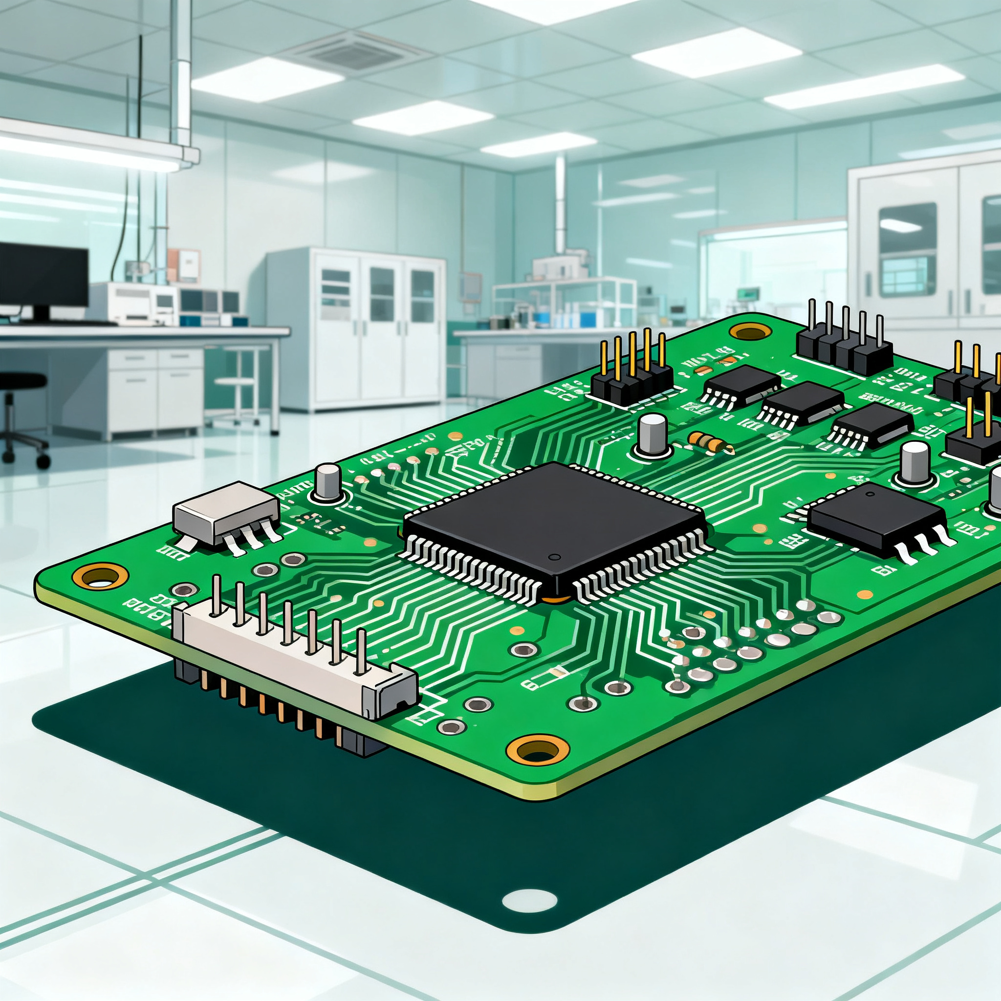
These numbers only hold meaning if the assembly environment is controlled. IPC Class II/III details from leading manufacturers confirm that even the most precise solder paste print can be ruined by a particle landing on a pad. That is why medical PCB assembly at NovaPCBA takes place inside an ISO 7 (Class 10,000) cleanroom with HEPA filtration, positive pressure, and continuous particle monitoring. Operators wear full gowning — gloves, hairnets, beard covers, and static‑dissipative smocks — not just to protect the board from contamination, but to maintain the ionic cleanliness levels that Class 3 demands.
IPC standards relevance is often underestimated until a board fails. A fabricator skipping IPC‑6012 tests might ship boards that pass initial visual inspection but delaminate after six months in the field. An assembler violating IPC‑A‑610 could let cold solder joints slip through, leading to warranty claims. In medical devices, non‑compliance is not just expensive — it is dangerous. IPC‑A‑600 acceptability criteria for bare boards are equally critical: a micro‑etch discrepancy that looks minor under the scope can become a latent short when ionic residues attract moisture. At NovaPCBA, every incoming bare board is inspected to IPC‑A‑600 Class 3 before it enters the cleanroom, and we maintain temperature (22 ± 2 °C) and humidity (40 ± 10% RH) to prevent moisture‑related delamination during reflow.
Tip: When you specify Class 3, insist on a pre‑production microsection for plated‑through holes. This sample will reveal whether the fabricator’s copper plating meets the 25 µm average and whether the via fill is void‑free — a critical check for boards that will undergo multiple thermal cycles.
ISO 13485, FDA, and the Paper Trail That Proves Your PCB Is Safe
Medical PCB assembly is not a standalone manufacturing step; it is a regulatory event. Every board that leaves a line destined for a medical device carries a burden of proof—proof that the laminate lot was correct, that the solder paste was within its shelf life, that the reflow profile matched the profile validated for that BOM, and that the inspection record was signed by a certified operator. These are not administrative niceties. They are the data points that populate a Design History File (DHF) and, when an FDA inspector walks in, the only thing standing between you and a Form 483.
Medical PCB guide resources emphasize that ISO 13485‑compliant manufacturing must connect every process output to a risk management file. At NovaPCBA, we implement this connection through a closed‑loop ERP system that records parameters from the stencil printer, pick‑and‑place, reflow oven, AOI, and X‑ray stations, all indexed to the unique board serial number. This is not a high‑level “batch” record; it is a per‑board digital thread that allows us to prove, for example, that board SN MED‑2341 received only components from the approved AVL and was reflowed with a profile that stayed within ±2 °C of the target peak.
ISO 13485 and IPC‑6012 together form the backbone of medical PCB acceptance. IPC‑6012 Class 3 defines the qualification and performance requirements for the bare board, including thermal stress coupons, cleanliness testing, and plating integrity. The compliance chain looks like this:
| Documentation Element | Standard Reference | What It Captures | Audit Value |
|---|---|---|---|
| Material certification | IPC‑4101, ISO 13485 §7.4 | Laminate type, glass transition temperature, CTE, flammability rating | Proves that the base material can withstand the sterilization method and operating temperature |
| Bare board acceptance | IPC‑6012 Class 3, IPC‑A‑600 Class 3 | Plating thickness, annular ring, solder mask registration, microsection | Confirms that the bare board meets the electrical and mechanical integrity needed for Class 3 soldering |
| Assembly process record | ISO 13485 §7.5.1, IPC‑J‑STD‑001 Class 3 | Print parameters, placement data, reflow profile, wave solder parameters | Demonstrates that every process step was executed within validated limits |
| Inspection and test data | IPC‑A‑610 Class 3, IPC‑6012 | AOI images, X‑ray images for BGAs, ICT results, flying probe data | Provides objective evidence that each board passed the acceptance criteria |
| BOM change control log | FDA 21 CFR Part 820.30, ISO 13485 §7.3.7 | Every substitution, its justification, and its link to affected serial numbers | Enables precise recall scoping and proves that changes were reviewed for risk |
Standards overview documents often note that the weakest link in the chain is not the manufacturing floor but the transition between design and production. When a component is substituted during a shortage, an engineer might approve it over email. Without a formal change order that flows into the ERP and updates the DHF, that substitution becomes a ticking time bomb. At NovaPCBA, we treat every BOM change as a mini‑design review. The substitute is tested for form, fit, and function, and the decision is captured in the device master record with a unique change number. Only then is the BOM updated in the production system, and the new lot code is linked to the serial numbers of the boards that receive it. This discipline is what makes a DHF audit‑ready and, more importantly, what keeps a recall small.
Designing for Medical PCB Assembly: Traceability, Test Points, and Supplier Vetting
The best assembly process in the world cannot rescue a board that was designed without considering the realities of high‑reliability manufacturing. Engineers who have not built medical products before often make the same three mistakes: they omit test points for in‑circuit testing, they select materials that cannot survive repeated sterilization, and they assume that any EMS provider with a cleanroom can handle Class 3. The following design practices, drawn from our experience at NovaPCBA, will keep your board out of the re‑spin loop.
- Provide a test point for every net. IPC Class 3 requires 100% electrical verification of the assembly. In‑circuit testing (ICT) or flying probe testing is the only practical way to achieve this. Leave at least one 0.9 mm diameter test pad per net, accessible from the bottom side, and avoid placing test points under tall components. Without this, you force the assembler to use boundary scan alone, which cannot catch passive component failures.
- Choose materials with CTE values that match the assembly’s thermal profile. A board that will be sterilized in an autoclave at 134 °C must use a laminate with a glass transition temperature (Tg) above 170 °C and a Z‑axis CTE below 50 ppm/°C. Polyimide or high‑Tg FR‑4 is often necessary. Thin dielectrics and fine geometries pose additional challenges: when you push below 75 µm trace/space, X/Y dimensional stability becomes critical, and the fabricator must provide a tight impedance tolerance.
- Specify via tenting or via fill for cleanliness. Open vias can trap flux residues and cause ionic contamination spikes. For Class 3 medical boards, we recommend IPC‑4761 Type II or Type III via protection (non‑conductive epoxy fill and over‑plate) to eliminate hidden contamination pockets.
- Vet your assembly partner against more than a price quote. Supplier selection guides rightly emphasize that medical PCB assembly requires process control, engineering support, and traceability infrastructure that far exceed what a generalist EMS can offer. Ask to see the cleanroom particle count logs, the training records for IPC‑A‑610 Class 3 inspectors, and a sample lot‑traceability report. If the provider cannot produce a per‑board thermal profile and a complete BOM‑to‑serial‑number map, they are not ready for medical.
Design and cost factors for medical PCBs are heavily influenced by the testing and documentation overhead. A Class 3 board may cost 15‑25% more than a Class 2 equivalent, but that premium largely disappears when you compare it to the cost of a single recall. The table below captures the key supplier vetting criteria that we recommend engineers use when evaluating a potential medical PCB assembly partner.
| Vetting Criterion | What to Ask | Red Flag | NovaPCBA Standard |
|---|---|---|---|
| Cleanroom classification | “What ISO class is your SMT area, and can you share the last 30 days of particle count data?” | “Our whole floor is clean” — no ISO certification or log | ISO 7 (Class 10,000) with continuous monitoring; logs available for audit |
| Traceability depth | “Can you trace a single component on a board back to its reel lot code and the BOM revision?” | Traceability stops at the batch level; no per‑board serialization | Per‑board, per‑component lot traceability linked to ERP and DHF |
| IPC inspector certification | “Are your AOI programmers and visual inspectors certified to IPC‑A‑610 Class 3?” | “Our operators are trained” — no certification records | All inspectors hold current IPC‑A‑610 Class 3 and J‑STD‑001 certifications |
| Microsection capability | “Do you perform in‑house microsection for plating and solder joint evaluation?” | “We send samples out when needed” — adds weeks and decouples from process control | In‑house microsection lab; one sample per lot checked for PTH and via fill |
| BOM change management | “How do you handle an AVL substitution during a shortage, and how is it linked to the DHF?” | “We just swap the part and note it in the traveler” | Formal Engineering Change Order with justification, review, and serial‑number linkage |
When you design a medical PCB, you are not just laying out copper; you are creating a record that will be scrutinized years after the product ships. The most successful projects we have assembled at NovaPCBA are those where the engineer engaged us early, sharing the BOM and the stackup before releasing the design. That upfront collaboration catches issues like a via pad that is too small for the required annular ring, or a solder mask dam that is too thin for the fine‑pitch BGA, long before they become a recall driver.
Medical PCB Assembly FAQs: What Engineers and Buyers Need to Ask
Q: How does NovaPCBA ensure full component‑level traceability for medical PCB assemblies?
A: We assign unique lot codes to every component, reel, and bare board panel. During assembly, our ERP system logs the placement data, solder profile, and inspection results for each board’s serial number. This creates a digital thread that links every component to its original lot, the BOM revision it was built under, and the exact process parameters it experienced. If a recall becomes necessary, we can scope the affected population down to the individual serial number, avoiding the 10× over‑recall that plagues manufacturers with batch‑level traceability.
Q: What is the real cost difference between IPC Class 2 and Class 3 for a typical medical device PCB?
A: For a medium‑complexity PCB (8‑12 layers, 0.8 mm BGA pitch, moderate component count), Class 3 assembly typically adds 15–25% to the total assembly cost. The increase comes from higher‑reliability laminate materials, extended reflow profiling, 100% AOI and X‑ray, and microsection testing on a per‑lot basis. However, when you weigh that against the average cost of a Class I medical device recall — which can exceed $5 million — the Class 3 premium is negligible. Most of our medical customers treat it as cheap insurance.
Q: What cleanroom classification is required for medical PCB assembly, and how does it affect yield?
A: ISO 7 (Class 10,000) is the de facto minimum for medical device PCB assembly. At NovaPCBA, we operate to ISO 7 with HEPA‑filtered vertical laminar flow, positive pressure, and humidity control at 40 ± 10% RH. Controlling particulates below 10 µm and maintaining stable temperature and humidity prevent two of the biggest yield killers in medical assembly: solder balling from moisture‑laden components and ionic contamination bridges that cause latent failures. We see first‑pass yield improvements of 3‑5% compared to uncontrolled environments, which translates directly into higher reliability and fewer field returns.
Q: When should I specify IPC‑A‑600 Class 3 vs. IPC‑6012 Class 3 for my board?
A: You need both. IPC‑A‑600 Class 3 defines the visual acceptance criteria for bare boards — the workmanship standard that an inspector uses to judge whether a board is acceptable. IPC‑6012 Class 3 is the performance specification that defines the qualification and conformance testing requirements: thermal stress, plating thickness, ionic cleanliness, and microsection. For any medical device, your bare board purchase order should reference IPC‑6012 Class 3, and the acceptance criteria should be IPC‑A‑600 Class 3. At NovaPCBA, we enforce this dual requirement for every incoming lot, and we reject any board that fails the microsection coupon even if it looks good under the microscope.
Q: How do you handle BOM changes during a component shortage without risking FDA compliance?
A: Every substitute is treated as a formal engineering change. The component is reviewed against the device master record for form, fit, and function, and if it passes, we generate a change order that documents the justification, the test results, and the approval signatures. This change order is linked to the specific serial numbers of the boards that will receive the substitute. The Design History File is updated so that an auditor can see exactly which devices used the alternate part and why. We never perform a “quiet substitution” — that single act is what turns a component shortage into a recall.
Q: What testing and inspection protocols are mandatory for Class 3 medical PCBs?
A: The minimum required for Class 3 medical PCBs includes 100% automated optical inspection (AOI) after reflow, X‑ray inspection for all BGA and QFN packages, in‑circuit testing (ICT) or flying probe testing for electrical verification, and microsection analysis on a sample basis to verify plating thickness, via fill, and solder joint integrity. At NovaPCBA, we augment these with ionic contamination testing to IPC‑TM‑650 2.3.25 and, for high‑reliability applications, thermal cycling on a sample of each lot to validate the assembly against the expected life profile. For implantable devices, we also perform C‑mode scanning acoustic microscopy to detect delamination invisible to X‑ray.
References & Further Reading
- Medical PCB Assembly & Manufacturing | IPC Class 3 · Full Traceability — QueenEMS article detailing the impact of traceability gaps on recall scope.
- Medical Device Recalls and Early Alerts | FDA — Official FDA database of medical device recalls.
- Medical Device Recall Trends 2024‑2026: Statistics and Root Causes — MedDeviceGuide analysis of recall surge and root causes.
- Medical Device Recall Statistics: 2026 Data — XS Supply compilation of 2026 recall data from FDA databases.
- Medical Device PCBs – IPC Class II and IPC Class III Specifications — Epec technical overview of IPC requirements and HALT/HASS testing.
- IPC Standards and Why They Matter in PCB Manufacturing — Microchip USA article on consequences of IPC non‑compliance.
- Medical Device PCB Assembly: Standards & Regulations for Quality and Safety — Accelerated Assemblies guide to IPC‑A‑600 and related standards.
- Medical PCB: Complete Guide to Design, Manufacturing & Assembly — PCBSync comprehensive guide for engineers and procurement teams.
Want to discuss your project?
Use the quick bar below or this form—we will route you to an engineer.
Contact us