Strategies for PCB Assembly Cost Reduction: Tips for 6-Layer Boards
Strategies for PCB Assembly Cost Reduction: Tips for 6-Layer Boards Introduction In the ever-evolving electronics industry, reducing costs while maintaining high quality is a constant challenge. For m...
Introduction
In the ever-evolving electronics industry, reducing costs while maintaining high quality is a constant challenge. For multi-layer boards, particularly 6-layer PCBs, achieving cost efficiency without compromising performance is crucial. This article delves into strategies for reducing assembly costs, focusing on PCB layout rules, stackup design, signal integrity, and manufacturing considerations. By implementing these strategies, designers and manufacturers can optimize their processes, enhance product reliability, and achieve significant cost savings.
Technical Overview
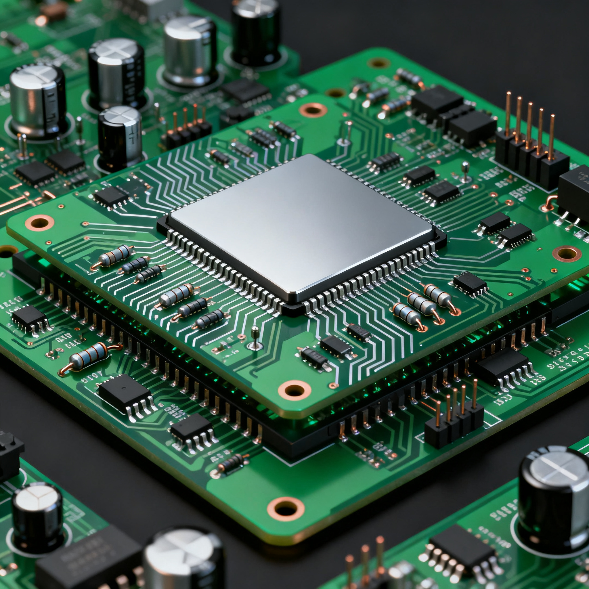
The design and assembly of 6-layer PCBs involve complex processes that require careful consideration of various technical aspects. The core concepts include understanding the architecture of multi-layer boards, principles of signal integrity, and the impact of design rules on manufacturing efficiency. Multi-layer boards allow for more intricate circuit designs, enabling higher component density and improved electrical performance. However, this complexity also demands meticulous planning in terms of layer stackup, trace routing, and material selection to ensure optimal performance and cost-effectiveness.
Signal integrity is a critical factor in PCB design, particularly for high-speed applications. Ensuring minimal signal loss and interference requires adherence to specific layout rules and careful selection of materials with favorable dielectric properties. Manufacturing considerations, such as panel utilization and assembly techniques, also play a significant role in cost reduction. By optimizing these elements, designers can achieve a balance between performance and cost, ultimately delivering a more competitive product.
Detailed Specifications
Understanding the detailed specifications of PCB design is essential for effective cost reduction. Key specifications include trace width, spacing, via sizes, and clearances, all of which influence the manufacturability and performance of the board. Adhering to industry standards, such as those outlined by IPC, ensures consistency and quality in PCB production. The following table provides an overview of critical PCB design rules that impact assembly costs and overall board performance.
| Design Parameter | Standard Value | Significance |
|---|---|---|
| Trace Width | 0.15 mm | Ensures current carrying capacity |
| Trace Spacing | 0.15 mm | Prevents short circuits |
| Via Diameter | 0.3 mm | Facilitates layer interconnections |
| Via Pad Size | 0.6 mm | Provides mechanical stability |
| Clearance | 0.2 mm | Minimizes risk of arcing |
| Annular Ring | 0.1 mm | Ensures via reliability |
| Solder Mask Clearance | 0.1 mm | Avoids solder bridging |
| Component Pad Size | 0.5 mm | Ensures proper solder joint |
| Drill to Copper | 0.3 mm | Prevents shorts with inner layers |
| Aspect Ratio | 8:1 | Ensures manufacturability of vias |
Key Takeaways from the Specifications
The specifications outlined in the table above are crucial for ensuring the manufacturability and reliability of 6-layer PCBs. Proper trace width and spacing are essential to prevent electrical shorts and ensure adequate current carrying capacity. Via sizes and annular rings are critical for mechanical stability and reliable electrical connections between layers. Adhering to these design rules not only enhances the performance of the board but also reduces the likelihood of manufacturing defects, thereby lowering overall costs.
| Layer Configuration | Description | Applications |
|---|---|---|
| Signal-Ground-Signal-Power-Signal-Ground | Standard configuration for balanced performance | General purpose, mixed-signal designs |
| Signal-Power-Ground-Signal-Power-Ground | Optimized for power distribution | Power-intensive applications |
| Ground-Signal-Power-Ground-Signal-Ground | Enhanced signal integrity | High-speed digital circuits |
| Power-Ground-Signal-Signal-Ground-Power | Improved EMI performance | RF and microwave applications |
| Signal-Signal-Ground-Power-Ground-Signal | Cost-effective with good performance | Consumer electronics |
| Ground-Power-Signal-Power-Ground-Signal | Balanced for mixed-signal | Telecommunications |
Practical Implications
The choice of layer stackup plays a significant role in the overall performance and cost of a 6-layer PCB. Different configurations offer varying benefits in terms of signal integrity, power distribution, and electromagnetic interference (EMI) management. For instance, configurations with dedicated ground and power planes enhance signal integrity and reduce EMI, which is critical for high-speed and RF applications. Selecting the appropriate stackup based on the specific requirements of the application can lead to substantial improvements in performance and cost savings.
| Material | Dielectric Constant (Dk) | Loss Tangent (Df) |
|---|---|---|
| FR-4 | 4.5 | 0.020 |
| Rogers 4350B | 3.48 | 0.0037 |
| Rogers 4003C | 3.55 | 0.0027 |
| Isola 370HR | 4.04 | 0.019 |
| Nelco N7000-2 | 3.7 | 0.009 |
| Panasonic Megtron 6 | 3.4 | 0.004 |
| Arlon 85N | 3.5 | 0.0035 |
| Taconic RF-35 | 3.5 | 0.0018 |
Application Guidelines
Material selection is a critical aspect of PCB design that affects both performance and cost. The dielectric constant (Dk) and loss tangent (Df) are key parameters that influence signal integrity and thermal performance. For high-frequency applications, materials like Rogers 4350B or Taconic RF-35 with low Dk and Df values are preferred due to their superior signal integrity and reduced signal loss. Conversely, for cost-sensitive applications, FR-4 remains a popular choice due to its affordability and adequate performance for many standard applications. Evaluating these material properties in the context of specific application requirements is essential for optimizing both cost and performance.
Design Considerations
When designing 6-layer PCBs, several practical guidelines can help achieve cost efficiency without sacrificing performance. First, optimizing the use of layers by strategically assigning signal, power, and ground planes can enhance signal integrity and reduce EMI. It's important to minimize the number of vias, as excessive vias can increase manufacturing complexity and cost. Additionally, careful routing of traces and maintaining uniform trace widths can prevent signal degradation and improve manufacturability.
The choice of materials also plays a significant role in cost reduction. While high-performance materials offer superior electrical properties, they can be expensive. Evaluating the trade-offs between material cost and performance can help in selecting the most appropriate material for the application. Furthermore, working closely with manufacturers to understand their capabilities and limitations can lead to better design decisions and cost savings.
Lastly, adhering to industry standards such as IPC-A-610 and IPC-2221 ensures consistency and quality, reducing the risk of rework and associated costs. By implementing these design considerations, engineers can develop 6-layer PCBs that meet performance requirements while remaining cost-effective.
Step-by-Step Implementation
- Define the application requirements: Begin by understanding the specific needs of your application, including electrical performance, environmental conditions, and cost constraints.
- Select the appropriate layer stackup: Choose a stackup configuration that balances signal integrity, power distribution, and EMI management based on the application's needs.
- Material selection: Evaluate materials based on dielectric properties, thermal performance, and cost. Choose a material that meets the application's requirements while being cost-effective.
- Adhere to design rules: Follow industry-standard design rules for trace widths, spacing, via sizes, and clearances to ensure manufacturability and performance.
- Optimize trace routing: Minimize the number of vias and maintain uniform trace widths to improve signal integrity and reduce manufacturing complexity.
- Collaborate with manufacturers: Work closely with PCB manufacturers to understand their capabilities and optimize the design for manufacturability.
- Perform design validation: Use simulation tools to validate the design's electrical performance and identify potential issues before fabrication.
- Iterate and refine: Based on validation results, make necessary adjustments to the design to address any identified issues and optimize performance.
Common Issues & Solutions
- Issue: Signal integrity problems due to improper routing.
Solution: Use controlled impedance routing and maintain consistent trace widths to minimize signal reflection and loss. - Issue: Excessive EMI affecting board performance.
Solution: Implement proper grounding techniques and use dedicated ground planes to shield sensitive circuits. - Issue: High manufacturing costs due to complex design.
Solution: Simplify the design by reducing the number of vias and optimizing layer stackup for manufacturability. - Issue: Inadequate thermal management leading to overheating.
Solution: Use materials with good thermal properties and design for adequate heat dissipation through proper layout and component placement. - Issue: Poor solder joint reliability.
Solution: Ensure proper pad sizes and solder mask clearances to facilitate reliable soldering during assembly. - Issue: Delays in production due to design errors.
Solution: Conduct thorough design reviews and simulations to identify and correct errors before fabrication.
Applications & Use Cases
6-layer PCBs are widely used across various industries due to their ability to support complex circuit designs while maintaining a compact form factor. In telecommunications, they enable high-speed data transfer and efficient power distribution in networking equipment. In consumer electronics, 6-layer boards provide the necessary complexity for advanced functionalities in smartphones and tablets. Additionally, in the automotive sector, they are used for sophisticated control systems that require reliable signal integrity and robust performance under harsh conditions. These examples highlight the versatility and importance of 6-layer PCBs in modern technology.
Selection & Sourcing Guide
When selecting and sourcing materials and components for 6-layer PCBs, it's important to consider factors such as cost, performance, and availability. Collaborating with reliable suppliers and manufacturers can ensure quality and timely delivery. For a comprehensive list of electronic components and suppliers, visit IC Online.
FAQ
- What is the primary advantage of using a 6-layer PCB?
The primary advantage is the ability to support complex circuit designs with improved signal integrity and power distribution. - How can I reduce the cost of a 6-layer PCB?
Optimize the layer stackup, minimize the number of vias, and select cost-effective materials without compromising performance. - What materials are recommended for high-frequency applications?
Materials like Rogers 4350B and Taconic RF-35 are recommended due to their low dielectric constant and loss tangent. - Why is signal integrity important in PCB design?
Signal integrity ensures reliable data transmission and minimizes errors in high-speed applications. - What role does layer stackup play in PCB performance?
Layer stackup affects signal integrity, power distribution, and EMI management, impacting overall board performance. - How can I ensure reliable solder joints?
Use proper pad sizes and solder mask clearances to facilitate effective soldering during assembly. - What are IPC standards, and why are they important?
IPC standards provide guidelines for PCB design and manufacturing, ensuring quality and consistency. - How do I choose between different dielectric materials?
Consider the application's frequency requirements, thermal performance, and cost constraints to select the most suitable material. - What is the impact of EMI on PCB performance?
EMI can cause interference and degrade signal quality, affecting overall board performance. - How can I improve thermal management in PCB design?
Use materials with good thermal properties and design for adequate heat dissipation through layout and component placement.
Conclusion
Designing and manufacturing 6-layer PCBs require careful consideration of various factors to achieve cost efficiency and high performance. By understanding and implementing the strategies discussed in this article, engineers can optimize their designs, reduce assembly costs, and deliver reliable products. The integration of thoughtful design practices, material selection, and adherence to industry standards will lead to successful PCB projects that meet both technical and financial objectives.