Strategies for PCB Assembly Cost Reduction in Advanced SMT Projects
Strategies for PCB Assembly Cost Reduction in Advanced SMT Projects Introduction In today's fast-paced electronics industry, reducing costs while maintaining quality is a critical challenge for PCB as...
Introduction
In today's fast-paced electronics industry, reducing costs while maintaining quality is a critical challenge for PCB assembly projects. As Surface Mount Technology (SMT) becomes the standard for high-density and complex PCB designs, it is crucial to adopt strategies that optimize both design and manufacturing processes. This article explores effective strategies for reducing PCB assembly costs in advanced SMT projects, focusing on PCB layout rules, stackup design, signal integrity, and manufacturing considerations.
Technical Overview
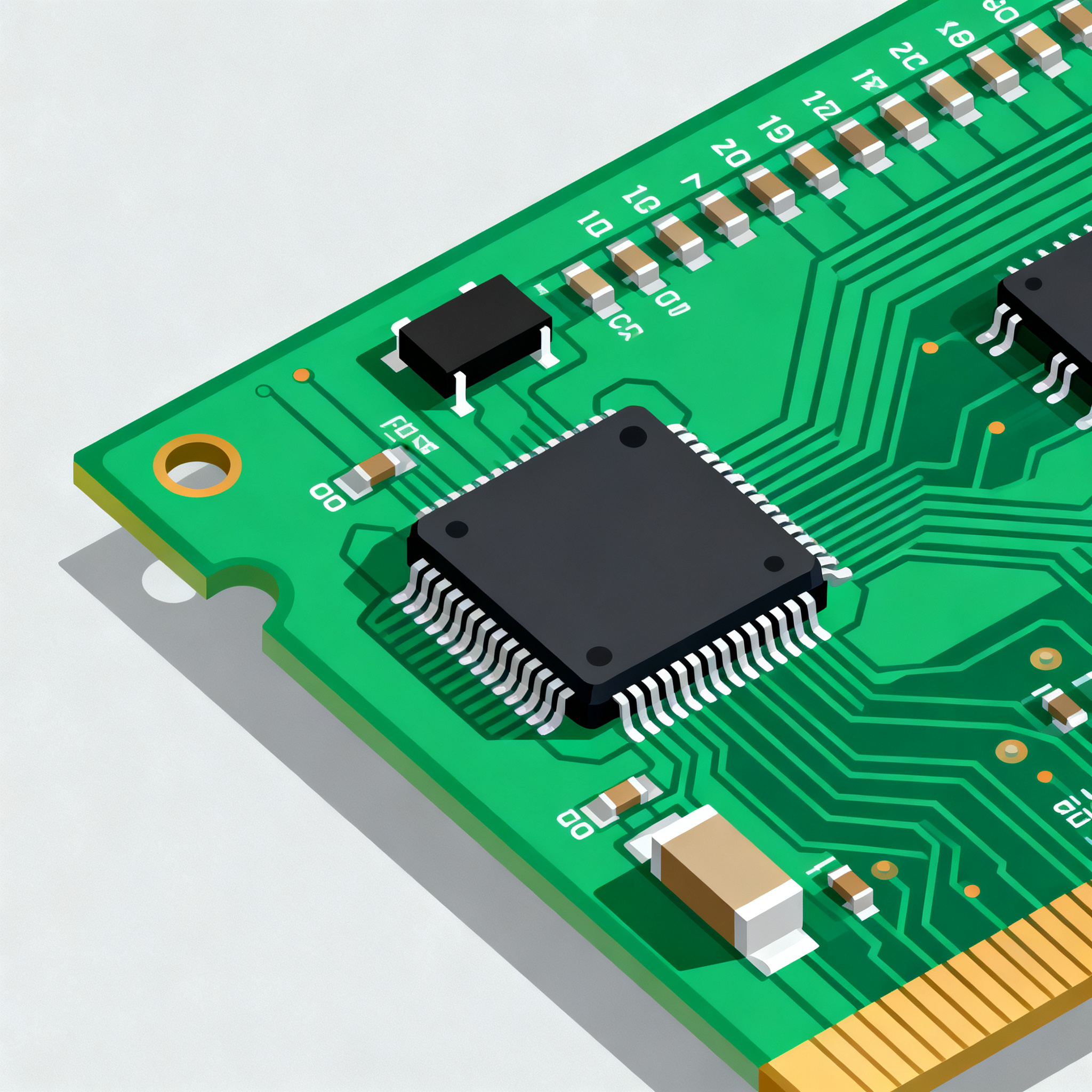
The core concepts of PCB design in advanced SMT projects revolve around achieving high performance with cost efficiency. This involves understanding the architecture of SMT components, the principles of signal integrity, and the implications of manufacturing techniques. SMT allows for smaller, lighter, and more efficient PCBs by mounting components directly onto the surface of the board. However, this also demands meticulous attention to design rules and manufacturing processes to avoid costly errors and rework. Key considerations include trace width and spacing, via sizes, and clearances, all of which affect the electrical performance and manufacturability of the PCB. By adhering to industry standards such as those outlined by IPC, designers can ensure that their PCBs meet quality and performance expectations while minimizing costs.
Detailed Specifications
In PCB design, adhering to specific design rules is essential to achieve optimal performance and manufacturability. These specifications include trace width, spacing, via sizes, and clearances, which directly impact the electrical characteristics and reliability of the PCB. Understanding these parameters allows designers to make informed decisions that balance performance with cost-effectiveness.
| Design Rule | Minimum Value | Recommended Value |
|---|---|---|
| Trace Width | 4 mil | 6-8 mil |
| Trace Spacing | 4 mil | 6-8 mil |
| Via Hole Size | 0.2 mm | 0.3 mm |
| Pad Size | 0.4 mm | 0.6 mm |
| Annular Ring | 0.1 mm | 0.15 mm |
| Clearance to Edge | 0.5 mm | 0.75 mm |
| Silkscreen Clearance | 0.1 mm | 0.2 mm |
| Component Spacing | 0.2 mm | 0.5 mm |
| Drill to Copper | 0.2 mm | 0.3 mm |
| Layer-to-Layer Spacing | 0.1 mm | 0.15 mm |
Key Takeaways from the Specifications
The data in the table above provides critical guidelines for ensuring that PCB designs meet both electrical and manufacturing requirements. For instance, adhering to minimum trace width and spacing values ensures signal integrity and reduces the risk of short circuits. Meanwhile, recommended values provide a buffer that enhances reliability and manufacturability. Understanding these specifications helps in selecting the appropriate design parameters that align with the capabilities of your manufacturing partner, thereby optimizing costs and reducing the risk of errors.
| Stackup Configuration | Layer Count | Applications |
|---|---|---|
| Single Layer | 1 | Simple circuits, low cost |
| Double Layer | 2 | Moderate complexity, increased routing |
| Four Layer | 4 | High-speed, moderate density |
| Six Layer | 6 | Advanced signal integrity |
| Eight Layer | 8 | Complex circuits, high density |
| Ten Layer | 10 | Very high-speed, RF applications |
| Twelve Layer | 12 | Ultra-complex designs, server boards |
Practical Implications
Selecting the appropriate layer stackup is crucial in advanced SMT projects, as it directly impacts the board's performance, size, and cost. Single and double-layer boards are cost-effective for simple applications, while multi-layer configurations like eight or ten layers are required for high-density and high-speed applications. Understanding the specific needs of your project and choosing the right stackup configuration can lead to significant cost savings and improved performance by optimizing the use of space and ensuring adequate signal integrity.
| Material | Dielectric Constant | Loss Tangent |
|---|---|---|
| FR-4 | 4.5 | 0.020 |
| Rogers 4003C | 3.55 | 0.0027 |
| Rogers 4350B | 3.66 | 0.0037 |
| Isola 370HR | 4.04 | 0.019 |
| Nelco N4000-13 | 3.9 | 0.016 |
| Polyimide | 3.5 | 0.004 |
| BT Epoxy | 4.2 | 0.015 |
| Ceramic | 9.8 | 0.001 |
| PTFE | 2.1 | 0.001 |
Application Guidelines
Choosing the right material for your PCB is essential for achieving the desired electrical performance and reliability. Materials like FR-4 are commonly used due to their balance of performance and cost. However, for high-frequency applications, materials like Rogers and PTFE offer superior dielectric properties and lower loss tangents. Selecting the appropriate material based on your project's requirements can enhance performance and reduce costs associated with signal loss and thermal management.
Design Considerations
Practical design guidelines are essential for ensuring that a PCB meets the performance and cost requirements of an advanced SMT project. Designers must consider factors such as component placement, trace routing, and thermal management. Effective component placement minimizes signal path lengths and reduces the potential for interference. Trace routing should adhere to the specified design rules to ensure signal integrity and manufacturability. Additionally, thermal management is critical in high-density designs to prevent overheating and ensure reliability. By incorporating these considerations into the design process, engineers can create PCBs that are both cost-effective and high-performing.
Step-by-Step Implementation
- Define Project Requirements: Clearly outline the performance, cost, and size requirements for your PCB.
- Select Appropriate Materials: Choose materials that meet electrical and thermal performance needs while staying within budget.
- Design PCB Layout: Use CAD tools to design the PCB layout, adhering to design rules and optimizing component placement.
- Conduct Signal Integrity Analysis: Simulate the design to ensure signal integrity and address potential interference issues.
- Optimize Layer Stackup: Select a stackup configuration that meets performance needs and minimizes costs.
- Review and Validate Design: Perform a thorough design review and validation to identify and correct any issues.
- Collaborate with Manufacturing Partner: Work closely with your manufacturing partner to ensure the design is manufacturable.
- Prototype and Test: Create prototypes and conduct testing to verify performance and identify areas for improvement.
Common Issues & Solutions
- Issue: Signal Integrity Problems
Solution: Use proper trace width and spacing, and conduct signal integrity analysis during the design phase. - Issue: Thermal Management Challenges
Solution: Implement thermal vias and use materials with good thermal conductivity to dissipate heat. - Issue: Manufacturing Defects
Solution: Adhere to IPC standards and collaborate closely with your manufacturing partner to ensure quality. - Issue: Component Placement Errors
Solution: Optimize component placement to reduce signal path lengths and avoid interference. - Issue: Cost Overruns
Solution: Carefully select materials and stackup configurations that meet requirements without exceeding the budget. - Issue: Prototyping Delays
Solution: Work with quick-turn PCB assembly services to expedite prototyping and testing phases.
Applications & Use Cases
Advanced SMT projects are used in a variety of applications, including consumer electronics, telecommunications, automotive systems, and aerospace technologies. In consumer electronics, SMT allows for the miniaturization of devices, leading to more compact and portable products. In telecommunications, high-speed and high-frequency PCBs are essential for reliable signal transmission. Automotive systems benefit from SMT by enabling the integration of complex electronic systems into vehicles. In aerospace, the reliability and performance of SMT-based PCBs are critical for mission-critical applications.
Selection & Sourcing Guide
When selecting and sourcing components for your PCB, it is important to consider factors such as availability, cost, and compatibility with your design. Utilize resources like IC Online to find and compare components from multiple suppliers. This ensures that you have access to the best options for your project while staying within budget.
FAQ
- Q: What is the importance of trace width in PCB design?
A: Trace width is crucial for determining the current-carrying capacity and signal integrity of a PCB. Proper trace width prevents overheating and ensures reliable signal transmission. - Q: How can I reduce PCB assembly costs?
A: Optimize design for manufacturability, select cost-effective materials, and collaborate with your manufacturing partner to identify cost-saving opportunities. - Q: What role do IPC standards play in PCB design?
A: IPC standards provide guidelines for quality and reliability in PCB design and manufacturing, ensuring that designs meet industry best practices. - Q: Why is signal integrity important in high-speed designs?
A: Signal integrity is critical in high-speed designs to prevent data loss, signal distortion, and interference, which can affect the performance of the PCB. - Q: How do I choose the right stackup configuration?
A: Consider the complexity, performance requirements, and cost constraints of your project when selecting a stackup configuration. - Q: What are the advantages of using advanced materials like Rogers?
A: Advanced materials like Rogers offer lower dielectric constants and loss tangents, improving signal performance in high-frequency applications. - Q: How can I ensure my PCB design is manufacturable?
A: Follow design-for-manufacturability (DFM) guidelines and collaborate with your manufacturing partner to identify potential issues early in the design process. - Q: What is the benefit of using quick-turn PCB assembly services?
A: Quick-turn PCB assembly services expedite the prototyping and testing phases, allowing for faster iteration and time-to-market. - Q: How does component placement affect PCB performance?
A: Proper component placement minimizes signal path lengths and reduces the potential for interference, improving overall PCB performance. - Q: What are the common causes of manufacturing defects in PCBs?
A: Manufacturing defects can result from poor adherence to design rules, inadequate quality control, and miscommunication with manufacturing partners.
Conclusion
Reducing PCB assembly costs in advanced SMT projects requires a comprehensive approach that encompasses design, material selection, and collaboration with manufacturing partners. By adhering to industry standards, optimizing design parameters, and selecting the right materials and stackup configurations, engineers can achieve significant cost savings while maintaining high performance and reliability. These strategies not only enhance the competitiveness of your products but also ensure their success in the market.