Step-by-Step Tutorial: High-Reliability 4-Layer Rigid-Flex PCB Assembly for Wearable Medical Sensors
Step-by-Step Tutorial: High-Reliability 4-Layer Rigid-Flex PCB Assembly for Wearable Medical Sensors Why Wearable Medical Sensors Demand a New Level of PCB Assembly Reliability Wearable medical sensor...
Step-by-Step Tutorial: High-Reliability 4-Layer Rigid-Flex PCB Assembly for Wearable Medical Sensors
Why Wearable Medical Sensors Demand a New Level of PCB Assembly Reliability
Wearable medical sensors—ECG patches, continuous glucose monitors, pulse oximeter rings—operate in one of the most unforgiving environments for electronics: the human body. They are subjected to thousands of dynamic bending cycles daily, constant exposure to sweat and humidity, and temperature fluctuations from ambient to body heat. A rigid PCB with cables or connectors simply cannot survive this mechanical and environmental stress without intermittent failures that put patient data at risk.
Rigid-flex technology has become the architecture of choice precisely because it eliminates the failure-prone interconnects between rigid boards and flexible circuits. Instead, the flexible polyimide layers are an integral part of the stackup, transitioning seamlessly into FR-4 rigid sections. This monolithic construction distributes stress across the entire assembly and allows the device to conform to the body while keeping high-density components on stable rigid islands.
Consider the case of a cardiac monitoring patch described by Aivon: a 4‑layer rigid‑flex design with dynamic bends was able to withstand thousands of flex cycles without trace cracking or pad lifting¹. That level of endurance is not achievable with a conventional rigid board connected to a separate flexible printed circuit (FPC) via a ZIF connector—a configuration that introduces multiple mechanical interfaces and signal integrity challenges.
The thermal behavior of the materials further underscores why rigid‑flex demands a different assembly mindset. Polyimide heats and cools differently than FR‑4. As NextPCB notes, the thermal ramp‑up during reflow must be adjusted because polyimide’s heat transfer characteristics differ significantly from those of standard rigid laminates². If you treat a rigid‑flex board like a standard FR‑4 assembly, you risk delamination, warpage, and latent solder joint weaknesses that only appear after the device has been on a patient for weeks.
In short, the reliability requirements of wearable medical sensors force engineers and buyers to rethink every step—from material selection and stackup design to assembly profiling and inspection. This tutorial walks you through that process, focusing on a high‑reliability 4‑layer rigid‑flex PCB assembly that can meet the demands of body‑worn medical devices.
Inside a 4-Layer Rigid-Flex Stackup: Materials, Layer Bonding, and Assembly Process Flow
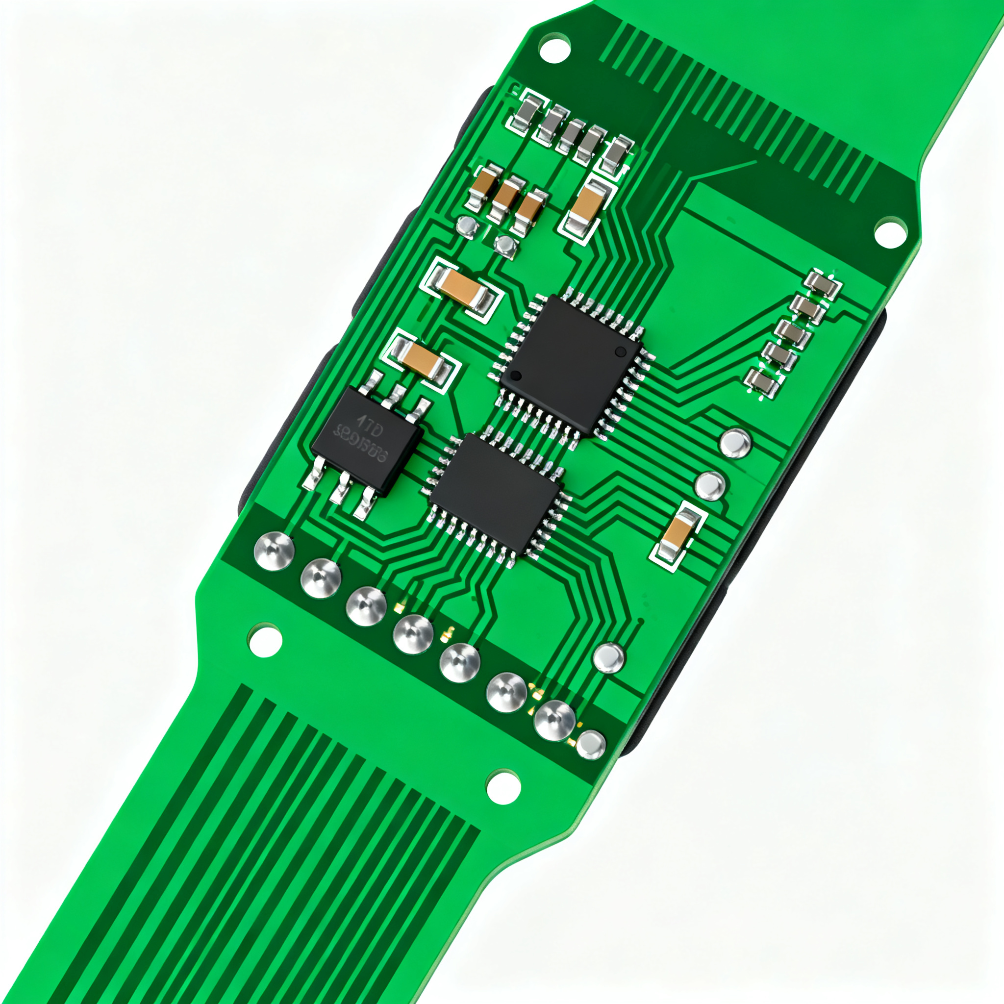
Before you can assemble a reliable rigid‑flex board, you need to understand what you are actually building. A typical 4‑layer rigid‑flex stackup for a wearable sensor consists of two rigid FR‑4 sections connected by a flexible polyimide core. The rigid areas provide mechanical support for components, while the flex layers carry signals across the bending zone without connectors.
The flexible core is usually a polyimide film (such as DuPont™ Kapton®) clad with rolled‑annealed copper. The rigid sections are built up with FR‑4 prepregs and copper foils laminated on either side of the flex core. The critical bonding material is a no‑flow or low‑flow epoxy prepreg that prevents resin from bleeding into the flex area during lamination. As HemeixinPCB explains, an epoxy pre‑preg bonding film is used to attach the inner layers together³. If the wrong prepreg is chosen, excess resin can flow into the bend region, stiffening it and creating a stress concentration that leads to early cracking.
The table below compares the key material properties that govern assembly behavior and field reliability.
| Property | Rigid Section (FR‑4) | Flex Section (Polyimide) | Impact on Assembly & Reliability |
|---|---|---|---|
| Glass Transition Temperature (Tg) | 130–170°C (standard FR‑4) | >250°C (polyimide) | Polyimide remains stable through multiple reflow cycles; FR‑4 softens, requiring careful thermal profiling to avoid warpage. |
| CTE (X‑Y axis) | 14–16 ppm/°C | 12–20 ppm/°C (adhesive‑based), 20–30 ppm/°C (adhesiveless) | CTE mismatch between rigid and flex can cause via barrel cracking if the transition zone is not properly designed. |
| Thermal Conductivity | 0.3–0.4 W/m·K | 0.12–0.2 W/m·K | Polyimide dissipates heat more slowly; ramp rates must be reduced to avoid thermal shock and delamination. |
| Moisture Absorption | 0.1–0.2% (24 h immersion) | 0.4–2.8% (depending on adhesive system) | Higher moisture uptake demands a pre‑bake before reflow to prevent popcorn effects in the flex layers. |
| Dielectric Constant (1 MHz) | 4.2–4.8 | 3.2–3.8 | Lower Dk in flex reduces signal delay; impedance control must account for the transition between rigid and flex dielectrics. |
| Flexural Endurance (dynamic) | Not applicable (rigid) | >100 million cycles (depending on bend radius) | Defines the minimum bend radius; IPC‑2223 recommends 10× the flex thickness for dynamic applications. |
The manufacturing sequence for a 4‑layer rigid‑flex board follows a disciplined flow that differs from standard rigid PCB fabrication. First, the inner flexible layers are patterned and etched. A coverlay—a polyimide film with a thin adhesive—is laminated over the flex traces, leaving openings only for pads that will connect to the rigid sections. Next, the rigid prepregs and outer copper foils are stacked on either side of the flex core, and the entire book is laminated under heat and pressure. After lamination, through‑holes are drilled, plated, and the outer layers are imaged and etched. The final steps include solder mask application on the rigid areas, surface finish deposition, and routing to release the flexible sections⁴. For HDI‑capable stackups, laser‑drilled microvias can be added to the outer layers, as detailed in the Würth Elektronik flex design guide⁵.
Tip: Always specify no‑flow prepregs in the rigid‑flex transition zone. Even a small amount of resin bleed can turn a flexible hinge into a brittle fracture point.
Rigid-Flex vs. Rigid Board with FPC Connectors: Which Architecture Survives on the Body?
When you are designing a wearable sensor, you have two main architectural choices: a single 4‑layer rigid‑flex assembly that integrates the flex layers directly into the board, or a rigid PCB connected to a separate flexible printed circuit (FPC) through a connector. On paper, the rigid‑plus‑FPC approach looks cheaper and simpler—you can use standard rigid PCB fabrication and buy off‑the‑shelf FPC cables. But on the body, the differences in reliability, assembly complexity, and total cost of ownership are stark.
The table below compares the two architectures across the metrics that matter most for a medical wearable that must survive daily bending, moisture, and vibration.
| Comparison Metric | 4‑Layer Rigid‑Flex Assembly | Rigid PCB + FPC with Connector | Selection Criteria & Failure Boundary |
|---|---|---|---|
| Dynamic Bend Reliability | Monolithic flex layers; no connector interface. Can exceed 100k cycles if bend radius ≥10× flex thickness⁶. | Connector is the weak point; contact fretting and intermittent opens after a few thousand cycles. FPC stiffener can crack at the termination. | For any application with repeated bending (arm patch, chest strap), rigid‑flex is mandatory. Connector‑based builds fail early in dynamic tests. |
| Assembly Complexity & Yield | Single assembly step; no manual connector mating. Reduced wiring eliminates cable assembly errors⁶. | Multiple assembly steps: solder connector on rigid PCB, attach FPC, mate. Risk of bent pins, misalignment, and ESD damage during handling. | Rigid‑flex simplifies the BOM and reduces labor; higher first‑pass yield for medium‑ to high‑volume medical builds. |
| Signal Integrity | Controlled impedance across the entire flex region; no impedance discontinuities from connectors. | Connector introduces a stub and impedance mismatch, especially for high‑speed sensor interfaces (SPI, I²C at fast mode). | For analog sensor front‑ends or digital buses above 10 MHz, rigid‑flex preserves signal quality. |
| Coverlay / Delamination Risk | Coverlay setback must be precisely controlled. If coverlay adhesive extends into the rigid section, soldering temperatures can cause delamination¹. | No coverlay in rigid area; delamination risk is limited to FPC stiffener bond. However, connector solder joints can crack under vibration. | Rigid‑flex requires strict DFM rules for coverlay openings, but the risk is manageable with teardrop‑shaped openings and proper setback. |
| Total Cost of Ownership | Higher NRE and unit cost, but eliminates connectors, cables, and rework. Fewer field returns in medical applications. | Lower initial PCB cost, but total system cost rises with connector, FPC, assembly labor, and potential warranty claims. | For Class III medical wearables, the lifecycle cost of rigid‑flex is often lower when reliability and patient safety are weighted. |
The coverlay delamination warning from Aivon is particularly instructive. If the coverlay extends too far into the rigid section, the adhesive can soften during reflow and create a path for moisture ingress later. The rigid‑flex approach forces you to manage this risk through design rules, but once those rules are followed, the resulting assembly is far more robust than any connector‑based alternative. As the AllPCB form factor face‑off notes, polyimide materials can endure temperatures up to 200°C and absorb vibrations better than rigid boards⁶—attributes that directly translate to longer life on the body.
Designing and Assembling Your Wearable Sensor Rigid-Flex: A Step-by-Step Checklist
Translating the physics of rigid‑flex into a reliable assembly requires a disciplined design and manufacturing workflow. The following five steps capture the critical decisions that separate a board that survives 100,000 flex cycles from one that cracks during the first week of a clinical trial.
- Define the bend radius and route traces with curves, not angles. The minimum dynamic bend radius should be at least 10× the total flex thickness. For a 0.2 mm flex core, that means a 2 mm radius. Always use curved traces in the bend area; 45‑degree angles act as stress concentrators that initiate copper cracking¹. Route traces perpendicular to the bend axis to minimize strain.
- Restrict fine‑pitch BGAs and heavy components to rigid sections. If a component must be placed on the flex area—for example, a tiny accelerometer near the skin—bond an FR‑4 or polyimide stiffener underneath to prevent solder joint cracking. NextPCB’s assembly guide explicitly recommends prioritizing high‑density components on rigid sections and using stiffeners when flex placement is unavoidable². Even with a stiffener, eliminate dynamic bending in that zone.
- Adjust the reflow profile for polyimide’s thermal behavior. Polyimide heats more slowly and retains heat differently than FR‑4. Ramp rates should be limited to 1–2°C/s, and peak temperatures must be carefully controlled to avoid blistering of the coverlay adhesive. Run a thermal profiling study on the actual stackup; standard FR‑4 profiles often cause delamination or warpage². A slower, more uniform profile also reduces the risk of voiding in the no‑flow prepreg bond line.
- Specify coverlay setback and teardrop openings. Keep the coverlay adhesive at least 0.25 mm inside the rigid‑flex transition zone. Never let it extend into the rigid area where soldering temperatures can weaken the bond. Use teardrop‑shaped openings around pads; sharp corners in the coverlay act as stress risers that can initiate delamination during thermal cycling¹.
- Inspect with X‑ray and AOI, not just visual checks. Hidden defects such as voids in the lamination bond line, micro‑cracks in plated through‑holes at the rigid‑flex interface, and insufficient solder under BGAs are invisible to the naked eye. The AllPCB step‑by‑step guide highlights the importance of automated optical inspection and X‑ray for rigid‑flex assemblies⁷. For medical wearables, 2D X‑ray and cross‑sectioning of first‑article samples should be mandatory.
The checklist below distills these steps into a quick‑reference DFM review that an engineer or buyer can use before releasing a design to fabrication.
| Checkpoint | Requirement | Verification Method |
|---|---|---|
| Bend radius | ≥10× flex thickness; curved traces only | CAD measurement; IPC‑2223 compliance check |
| Component placement | No BGAs on unsupported flex; stiffener thickness ≥0.2 mm if unavoidable | Design review; mechanical simulation of bend zone |
| Coverlay openings | Teardrop shape; adhesive setback ≥0.25 mm from rigid edge | Gerber overlay analysis; fabricator DFM report |
| Prepreg selection | No‑flow prepreg in transition zone; Tg >170°C for lead‑free reflow | Stackup documentation; material datasheet |
| Thermal profile | Ramp rate 1–2°C/s; peak 235–245°C (SAC305); profiling on actual stackup | Thermal couple data; post‑reflow cross‑section |
| Inspection | 100% AOI; X‑ray of all BGA and rigid‑flex vias; cross‑section on first‑article | Inspection report; IPC‑6013 class 3 criteria |
| Reliability testing | Dynamic bend cycling (≥10k cycles), thermal shock, 85/85 damp heat | Test plan aligned with IEC 60601‑1 risk management |
Following this checklist does not guarantee zero failures, but it systematically addresses the failure modes that have plagued wearable medical devices in the past. When you work with an assembly partner experienced in rigid‑flex, these requirements become part of the standard process flow, not afterthoughts. At NovaPCBA, we integrate these checks into our NPI process for medical rigid‑flex assemblies, ensuring that every build meets the reliability expectations of both the design team and the regulatory reviewer.
Wearable Medical Rigid-Flex Assembly: Questions Engineers and Buyers Ask
Q: What is the minimum dynamic bend radius for a 4-layer rigid-flex in a wearable patch?
A common rule is 10× the flex thickness for dynamic applications; for a 0.2 mm flex layer, that means ≥2 mm radius. Always validate with IPC‑2223 and physical cycling tests that mimic the patient’s movement. If your patch will be worn on a joint, consider a larger radius or a strain‑relief loop to prevent copper work‑hardening.
Q: How do I prevent coverlay delamination during assembly and use?
Keep coverlay adhesive well inside the rigid‑flex transition zone—never let it extend into the rigid area where soldering temperatures can weaken the bond. Use teardrop‑shaped coverlay openings and avoid sharp corners, as 45° angles act as stress concentrators. Additionally, specify a plasma clean before coverlay lamination to improve adhesion and reduce the risk of moisture‑driven delamination in the field.
Q: Can I mount a BGA or fine‑pitch component on the flexible portion?
It’s strongly discouraged. If unavoidable, bond a rigid stiffener (FR‑4 or polyimide) under the component to prevent solder joint cracking. Even then, dynamic bending should be eliminated in that zone by design. The stiffener must be thick enough to resist flexing—typically at least 0.3 mm—and the component should be placed away from the bend transition.
Q: What thermal profile adjustments are needed for polyimide flex layers?
Polyimide heats and cools differently than FR‑4. Ramp rates may need to be slowed to 1–2°C/s and peak temperatures carefully controlled to avoid blistering. Run a thermal profiling study on the actual stackup, as standard FR‑4 profiles often cause delamination or warpage. Also consider a nitrogen reflow environment to reduce oxidation of the exposed copper on the flex tails, which can degrade solderability.
Q: What reliability testing is required for medical wearable certification?
Beyond IPC‑6013 class 3, expect to perform dynamic bend cycling (thousands of cycles), thermal shock (-40°C to +85°C), and 85/85 damp heat testing. Document results for your IEC 60601‑1 risk management file, as the PCB assembly is a critical component in patient safety. Some notified bodies also ask for accelerated life testing that simulates one year of continuous wear, including sweat immersion and UV exposure.
Q: What are realistic lead times for a 4-layer rigid-flex prototype?
Standard quickturn is 8–12 working days, but medical‑grade builds with tighter trace/space and controlled impedance can extend to 15–20 days. Always confirm with the fabricator whether the stackup requires no‑flow prepregs and laser‑drilled microvias, which add 2–3 days. For first‑article builds that include cross‑sectioning and reliability coupons, plan for an additional week.
When you are ready to move from prototype to production, having an assembly partner that understands these nuances can compress the learning curve. NovaPCBA’s rigid‑flex assembly line is equipped with profile‑controlled reflow ovens, X‑ray inspection, and a dedicated medical device process team that can help you navigate the transition from design to a fully validated wearable sensor assembly.
References & Further Reading
- The Ultimate Guide to Rigid-Flex PCB Design – Aivon
- The Complete Guide to Rigid-Flex PCB Assembly – NextPCB
- Rigid Flex PCB Design Guidelines and Manufacturing – HemeixinPCB
- Rigid-Flex PCB Manufacturing Process Step by Step – HDI Circuit Board
- FLEX SOLUTIONS DESIGN GUIDE – Würth Elektronik
- PCB Form Factor Face-Off: Rigid vs. Flexible – AllPCB
- Mastering Rigid-Flex PCB Assembly: A Step-by-Step Guide for Engineers – AllPCB
- NovaPCBA – Rigid-Flex PCB Assembly Capabilities