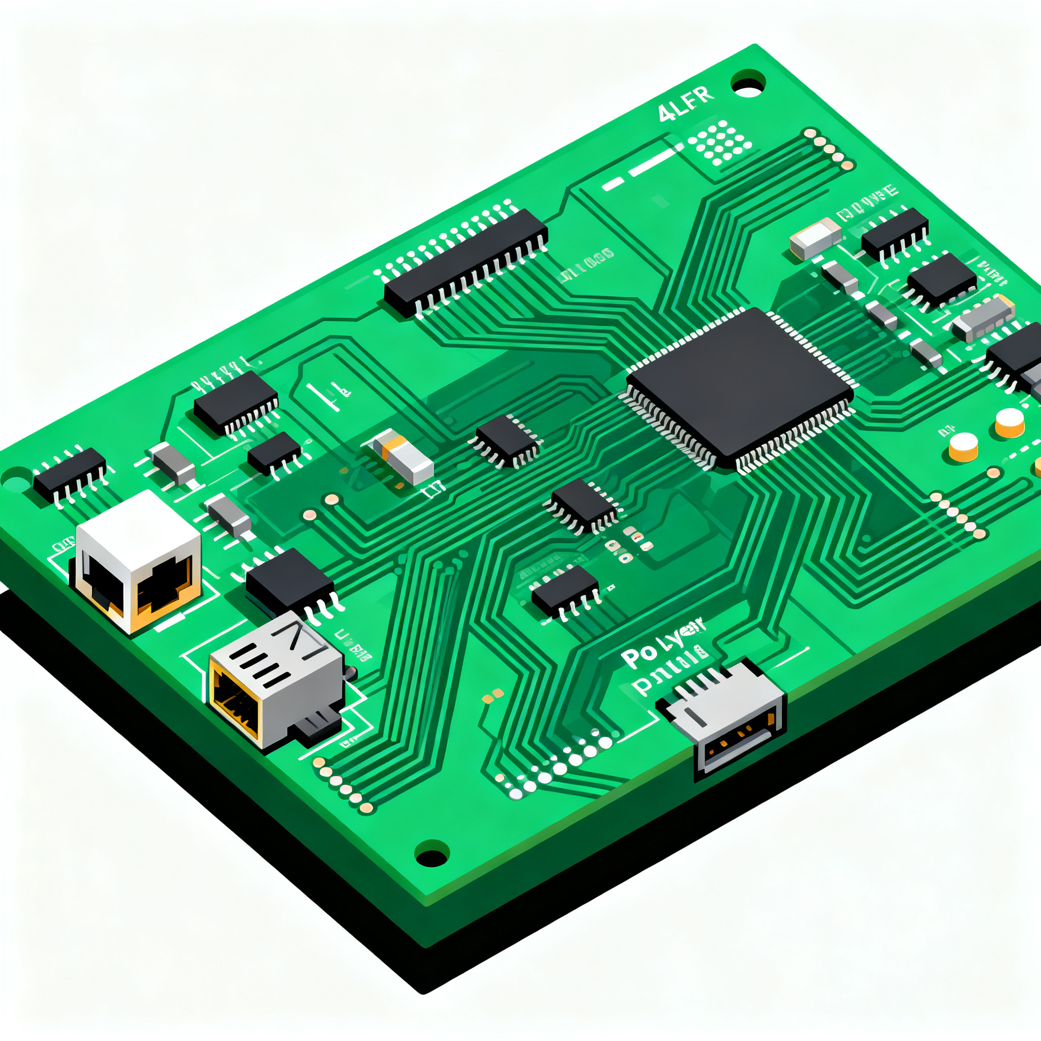
Step-by-Step Tutorial: Designing a 4-Layer Smart Security System PCB with Impedance Control and PoE Integration
Step-by-Step Tutorial: Designing a 4-Layer Smart Security System PCB with Impedance Control and PoE Integration Why 4-Layer Stackups Are No Longer Optional for PoE-Powered Security Devices Modern IP c...
Step-by-Step Tutorial: Designing a 4-Layer Smart Security System PCB with Impedance Control and PoE Integration
Why 4-Layer Stackups Are No Longer Optional for PoE-Powered Security Devices
Modern IP cameras, access control panels, and edge‑AI security sensors have moved far beyond simple motion detection. A single outdoor dome camera today streams 4K video at 30 fps, runs object classification on a neural network accelerator, and powers itself entirely through the Ethernet cable — all inside a sealed, fanless enclosure. That convergence of high‑resolution imaging, edge processing, and Power over Ethernet (PoE) has quietly pushed two‑layer PCB designs past their breaking point.
When you route Gigabit Ethernet differential pairs alongside a 25.5 W PoE power path on a two‑layer board, three problems become unavoidable. First, the return path for high‑speed signals is fragmented because there is no continuous reference plane; you end up with large current loops that radiate EMI and fail EN 55032 pre‑compliance scans. Second, the IR drop across thin 1 oz power traces can easily exceed 300 mV before reaching the load, starving the image sensor of clean voltage and introducing visible banding in low‑light scenes. Third, the lack of a dedicated ground plane makes it nearly impossible to maintain the 100 Ω differential impedance that the Ethernet PHY expects, leading to bit errors, link drops, and field returns.
This tutorial walks you through the complete design flow for a 4‑layer smart security PCB that integrates PoE (IEEE 802.3at Type 1 or Type 2), controlled‑impedance routing, and thermal management for sealed enclosures. You will learn how to select the right stackup, route differential pairs with length matching, handle the PoE DC‑DC converter layout, and avoid the DFM pitfalls that delay prototype builds. Along the way, we will reference the manufacturing expertise that Nova PCBA brings to complex boards like these — from impedance coupon testing to automated optical inspection of fine‑pitch PoE magnetics.
By the end, you will have a repeatable design methodology that delivers first‑pass success, not a series of costly respins. Let’s start with the physics that govern signal integrity and power delivery on a 4‑layer stackup.
How Impedance Control and PoE Power Delivery Shape Your Board’s Signal Integrity
Ethernet signals on a security camera board travel as differential pairs — typically 100 Ω differential impedance for 100BASE‑T and 1000BASE‑T. The PoE power path, on the other hand, carries up to 600 mA per pair (Mode A or Mode B) with a DC voltage of 44–57 V. Both coexist on the same RJ45 connector and, in a poorly designed stackup, can couple noise into the data lanes or create ground bounce that corrupts the PHY’s receiver eye diagram.
Controlled impedance is not a luxury; it is a physical requirement dictated by the dielectric constant (Dk) of the prepreg, the trace width, the trace spacing, and the distance to the nearest reference plane. The IPC‑2221 standard provides generic formulas, but every fabricator will fine‑tune the geometry based on their specific laminate and etching process. For a typical 4‑layer board using Isola FR408HR or a mid‑Tg FR‑4, the stackup in Table 1 yields a 100 Ω differential pair with a trace width of roughly 0.15–0.20 mm (6–8 mil) and a spacing of 0.15 mm (6 mil) when the prepreg thickness between Layer 1 and Layer 2 is 0.2 mm.
| Layer | Material / Thickness | Copper Weight | Function |
|---|---|---|---|
| L1 (Top) | 0.5 oz base + plating to 1 oz | 1 oz | High‑speed signals, PoE magnetics, PHY |
| Prepreg | FR‑4 2116, 0.2 mm (7.9 mil) | — | Dielectric for controlled impedance |
| L2 (Inner 1) | 0.5 oz (1 oz optional) | 0.5–1 oz | Solid ground plane (reference for L1) |
| Core | FR‑4, 0.71 mm (28 mil) | — | Mechanical rigidity, thermal mass |
| L3 (Inner 2) | 0.5 oz (1 oz optional) | 0.5–1 oz | PoE power plane (split if needed) |
| Prepreg | FR‑4 2116, 0.2 mm (7.9 mil) | — | Dielectric for bottom signals |
| L4 (Bottom) | 0.5 oz base + plating to 1 oz | 1 oz | Low‑speed signals, I²C, GPIO, thermal pads |
Table 1 — Typical 4‑layer stackup for a PoE security camera PCB with controlled 100 Ω differential pairs.
This configuration places a solid ground plane directly beneath the top‑layer differential pairs, providing an uninterrupted return path and tight coupling that keeps the differential impedance within ±10 % of 100 Ω. The PoE power plane on Layer 3 is separated from the ground plane by the thick core, which reduces plane‑to‑plane capacitance and minimizes the risk of power‑plane resonance coupling into the signal layers. If your design uses PoE+ (Type 2, 30 W) or PoE++ (Type 3/4, up to 90 W), consider increasing the copper weight on Layers 2 and 3 to 2 oz to handle the higher current density and to act as a heat spreader.
When you specify the stackup to your fabricator, always request an impedance coupon on the same panel. The coupon should replicate the exact trace geometry and dielectric spacing of your differential pairs. Nova PCBA includes TDR (Time Domain Reflectometry) testing on impedance coupons as part of their standard process for controlled‑impedance boards, giving you a measured report rather than a calculated estimate.
2-Layer vs. 4-Layer PCB: When the Cost Savings Backfire in Security Designs
On a bill of materials spreadsheet, a 2‑layer board looks attractive: the bare PCB cost is roughly 30–40 % lower than a 4‑layer equivalent, and the fabrication lead time can be a few days shorter. But for a PoE‑powered security device that must pass EMC, maintain a stable Ethernet link, and survive in an attic at 70 °C ambient, those upfront savings evaporate quickly. Table 2 compares the two approaches across the metrics that matter most in a security product.
| Comparison Metric | 2‑Layer PCB (No Dedicated Planes) | 4‑Layer PCB (GND + PWR Planes) | Selection Criteria & Failure Boundary |
|---|---|---|---|
| Signal return path | Fragmented; return current must flow through traces or stitching vias, creating large loops | Continuous ground plane on L2; return current flows directly under the signal trace | Choose 4‑layer when signal rise time < 1 ns or Ethernet link > 100 Mbps |
| 100 Ω differential impedance control | Difficult; impedance varies with nearby copper pours and board thickness, often > ±20 % | Predictable; impedance set by prepreg thickness and trace geometry, typically ±10 % | 2‑layer boards often fail IEEE 802.3 return loss masks; 4‑layer passes with margin |
| EMI radiated emissions | High loop area radiates common‑mode noise; ferrite beads and shielding add cost | Tight coupling to plane reduces loop area; often passes EN 55032 Class B without extra filtering | If the product is for residential use, 4‑layer avoids expensive shielding cans |
| PoE DC IR drop | Narrow power traces (e.g., 40 mil) drop 0.5–1 V at 600 mA, causing PD undervoltage lockout | Power plane on L3 has milliohm resistance; voltage drop < 50 mV | 2‑layer may require 4‑oz copper or bus bars, negating cost advantage |
| Thermal management | No internal copper to spread heat; hot spots around PoE IC and image sensor | Internal planes act as heat spreaders; thermal vias conduct heat to bottom layer | Sealed IP66 cameras need 4‑layer to keep junction temperatures below 125 °C |
| Design time & respin risk | Longer layout time to stitch grounds and manage return paths; higher probability of EMC failure | Shorter layout time; first‑pass success rate > 90 % for experienced designers | One failed EMC test can cost $10k–$20k in chamber time and redesign; 4‑layer pays for itself |
Table 2 — 2‑layer vs. 4‑layer comparison for a PoE security camera board.
Real‑world engineering teams have learned this lesson the hard way. A common scenario: a startup designs a 2‑layer PoE doorbell camera to hit a tight BOM target. The first prototypes link up in the lab, but when they enter the EMC chamber, the 125 MHz harmonics from the Ethernet PHY radiate 12 dB above the limit. The fix — adding copper tape, ferrite clamps, and a revised layout with a 4‑layer stackup — delays the product by three months and erases any per‑unit savings. The 4‑layer board, with its dedicated ground plane, would have passed on the first attempt.
If your design includes a high‑resolution image sensor (e.g., Sony STARVIS) that uses MIPI CSI‑2 lanes running at 1.5 Gbps per lane, a 2‑layer board is simply not an option. The MIPI differential impedance requirement (100 Ω) and the need for length matching across four lanes demand a controlled‑impedance stackup with a solid reference plane. In these cases, the 4‑layer board is not a cost adder; it is an enabler.
Routing Differential Pairs and Power Planes: A Layout Guide for First-Pass Success
With the stackup defined, you can now move into the physical layout. The following steps assume you are using a modern ECAD tool (Altium Designer, KiCad, Cadence Allegro) and have already placed the RJ45 jack, PoE magnetics, Ethernet PHY, and the main processor or SoC.
Step 1: Define the Stackup and Impedance Profile
Before drawing a single trace, configure the layer stack manager in your ECAD tool to match the agreed‑upon stackup from your fabricator. Enter the dielectric thickness, Dk, and copper weight for each layer. Create an impedance profile for 100 Ω differential pairs and assign it to the net class that includes the Ethernet TX and RX pairs. Most tools will automatically adjust the trace width and spacing when you route differential pairs on the top layer. Verify with a field solver such as the Saturn PCB Toolkit that the geometry yields 100 Ω ±10 %.
Step 2: Place the PoE Magnetics and PHY with Isolation in Mind
The PoE magnetics module (e.g., a discrete transformer and common‑mode choke, or an integrated RJ45 with magnetics) must sit as close as possible to the RJ45 connector. Keep the distance between the connector and the magnetics under 25 mm to minimize the loop area of the MDI (Medium Dependent Interface) traces. The Ethernet PHY should be placed on the opposite side of the magnetics, maintaining the isolation barrier required by IEEE 802.3. Route the differential pairs from the RJ45 to the magnetics, and from the magnetics to the PHY, as 100 Ω controlled pairs. Do not route any other signals through the isolation gap.
Step 3: Route 100 Ω Differential Pairs with Length Matching
Select the TX± and RX± pairs and route them as tightly coupled differential pairs on the top layer, referenced to the L2 ground plane. Maintain a consistent spacing between the two traces of each pair; a 6 mil gap is typical for a 6‑mil trace on a 0.2 mm prepreg. Avoid 90° corners — use 45° bends or arc routing. Keep the total length of each differential pair under 100 mm if possible, and length‑match the two traces within ±0.25 mm (10 mil) to minimize intra‑pair skew. For Gigabit Ethernet, also match the lengths of the TX and RX pairs to each other within 2.5 mm to meet the PHY’s timing budget.
When the differential pairs must change layers, place a stitching ground via within 1 mm of the signal vias to provide a continuous return path. Never route a differential pair across a split in the ground plane; if a split is unavoidable, bridge it with stitching capacitors (100 nF) on either side of the pair.
Step 4: Design the PoE Power Delivery Network
The PoE DC‑DC converter (e.g., an active bridge rectifier and a flyback or buck converter) should be placed close to the magnetics, on the isolated side. Use the inner Layer 3 as a solid power plane for the post‑converter voltage rail (e.g., 12 V or 5 V). Connect the PoE IC’s power pads to the plane with multiple thermal vias to spread heat into the internal copper. If your design uses a high‑current PoE++ scheme, consider using 2 oz copper on Layer 3 and stitching it to the bottom layer with an array of vias under the hot components.
Place the input bulk capacitor (100 µF electrolytic or 47 µF ceramic) directly at the output of the bridge rectifier, before the DC‑DC converter. This capacitor must withstand the full PoE voltage (57 V) and have low ESR to filter the switching noise. Keep the loop area between the rectifier, capacitor, and converter input as small as possible — aim for less than 50 mm².
Step 5: Stitch Ground Planes and Add Thermal Vias
Any area of the board not occupied by signals should be filled with ground copper on all layers and stitched with vias on a 5–10 mm grid. This stitching reduces EMI and improves thermal conductivity. Under the image sensor and the PoE controller, place a dense array of thermal vias (0.3 mm drill, 1.0 mm pitch) connecting the top‑layer thermal pad to the internal ground plane and the bottom‑layer copper pour. If the enclosure is metal, you can use the bottom copper as a conduction path to the housing.
Step 6: Run DFM Checks Before Releasing to Fabrication
Before generating Gerber files, run a comprehensive Design for Manufacturability (DFM) check. Pay special attention to:
- Acid traps: acute angles between traces and pads that can trap etchant and cause over‑etching.
- Annular rings: vias placed too close to the edge of a pad can break out during drilling; maintain at least 0.15 mm annular ring for controlled‑impedance vias.
- Solder mask dams: between fine‑pitch pads of the PoE magnetics (often 0.5 mm pitch), you need a solder mask dam of at least 0.1 mm to prevent bridging.
- Impedance discontinuities: check that no differential pair passes over a void in the reference plane.
Nova PCBA performs an automated DFM review on every order, flagging these issues before the board enters production. Their engineering team can also suggest stackup adjustments that bring the impedance within tolerance without increasing the per‑panel cost. Table 3 summarizes the key layout parameters you should verify against your fabricator’s capabilities.
| Parameter | Recommended Value | Fabricator Capability Check |
|---|---|---|
| Minimum trace width (outer layer) | 0.15 mm (6 mil) | Confirm etching tolerance ±10 % |
| Minimum spacing (outer layer) | 0.15 mm (6 mil) | Check for solder mask registration |
| Differential pair intra‑pair skew | < 0.25 mm (10 mil) | Verify with length tuning report |
| Impedance tolerance | 100 Ω ±10 % | Request TDR coupon test |
| Via annular ring (controlled‑impedance) | ≥ 0.15 mm (6 mil) | Ensure drill‑to‑copper clearance |
| Solder mask dam width | ≥ 0.1 mm (4 mil) | Verify for 0.5 mm pitch components |
| Copper‑to‑board edge clearance | ≥ 0.4 mm (16 mil) | Prevent exposed copper after routing |
| Thermal via drill diameter | 0.3 mm (12 mil) | Confirm aspect ratio < 8:1 |
Table 3 — Critical layout parameters for a 4‑layer PoE security PCB and the corresponding fabricator capability checks.
Following these six steps will dramatically reduce the number of prototype iterations. The combination of a well‑defined stackup, disciplined differential pair routing, and thorough DFM review is what separates a board that works on the bench from one that works in the field, year after year.
Smart Security PCB Design: Answers to the Questions Engineers Actually Ask
Q: What’s the smallest trace width I can reliably use for a 100 Ω differential pair on standard FR4?
Typically, you can use 6–8 mil traces with 6 mil spacing on a 4‑layer board where the prepreg between the top layer and the ground plane is 0.2 mm. The exact dimensions depend on the dielectric constant of the laminate (Dk ≈ 4.2–4.5 for standard FR‑4) and the copper weight (1 oz finished). If your fabricator uses a different prepreg, such as 0.15 mm 1080 glass, the required trace width may shrink to 4–5 mil, which pushes the limits of standard etching. Always confirm the geometry with a field solver or your fabricator’s impedance calculator before finalizing the layout. Nova PCBA provides a stackup design service that calculates the exact trace dimensions for their material set, removing the guesswork.
Q: My PoE security camera board runs hot in a sealed enclosure. How can I use the PCB to manage heat without a fan?
Start by specifying 2 oz copper for the internal ground and power planes; the thicker copper acts as a lateral heat spreader, moving thermal energy away from hot spots. Place a dense array of thermal vias (0.3 mm drill, 1.0 mm pitch) directly under the PoE controller’s exposed pad and under the image sensor’s thermal pad. These vias conduct heat to the bottom copper pour, which can be coupled to the aluminum enclosure with a thermal gap pad. For extreme cases, consider an aluminum‑backed PCB or a metal‑core PCB (MCPCB) for the LED driver section, while keeping the main logic on a standard 4‑layer FR‑4 board. Nova PCBA offers thermal management solutions that include metal‑core and heavy‑copper PCB fabrication, as well as assembly of thermal interface materials.
Q: When should I upgrade from standard FR4 to a high‑Tg laminate for a security panel?
If the board will operate at ambient temperatures above 110 °C or will undergo multiple lead‑free reflow cycles (e.g., for double‑sided assembly), a high‑Tg FR‑4 with a glass transition temperature above 170 °C is necessary. Standard FR‑4 (Tg ≈ 130–140 °C) can soften and delaminate under sustained high heat, causing via barrel cracks and impedance shifts. Outdoor security devices that use PoE+ (30 W) often reach internal temperatures of 90–100 °C in direct sunlight; a high‑Tg laminate provides a safety margin. Additionally, high‑Tg materials exhibit lower Z‑axis expansion, which improves plated‑through‑hole reliability over thermal cycling.
Q: How do I specify controlled impedance to my PCB manufacturer without overpaying for unnecessary tolerances?
On your fabrication drawing, clearly mark the differential pairs that require impedance control and state the target impedance and tolerance, e.g., “100 Ω ±10 %.” Provide a stackup table that lists the dielectric thickness and Dk for each layer. Do not request a tighter tolerance than your application needs; IPC‑2221 suggests ±10 % for most Ethernet applications, and tightening to ±7 % or ±5 % can increase the bare board cost by 20–50 % because the fabricator must sort panels by measured impedance. Nova PCBA’s engineering team can review your stackup and recommend the most cost‑effective tolerance that still meets the PHY’s return loss specification.
Q: Can I route PoE power and Ethernet signals on the same inner layer, or do I need separate planes?
You can route them on the same layer if you maintain adequate isolation — at least 3 mm between the high‑voltage PoE traces and the low‑voltage signal traces — but it is far safer to dedicate one inner layer to the PoE power plane and keep the differential pairs on the outer layers, referenced to a solid ground plane on the adjacent inner layer. This approach minimizes crosstalk, simplifies the return current path, and prevents common‑mode noise from coupling onto the Ethernet pairs. If board size constraints force you to mix power and signals on the same inner layer, use a split plane with a keep‑out zone and stitch the ground planes on either side of the split with capacitors.
Q: What DFM pitfalls do engineers overlook when designing 4‑layer security boards?
The most common oversights include: acid traps formed by acute angles where traces meet pads, which can cause over‑etching and opens; insufficient annular rings on vias used for controlled‑impedance transitions, leading to breakout and impedance spikes; and missing solder mask dams between the fine‑pitch pads of PoE magnetics, which results in solder bridging during assembly. Another frequent mistake is failing to define a clear keep‑out zone around the board edge, which can expose copper after depaneling. Nova PCBA’s pre‑production DFM review catches these issues and provides a detailed report with recommended corrections, often saving weeks of debugging and the cost of a second prototype run.
References & Further Reading
- IPC — Association Connecting Electronics Industries — IPC‑A‑610 and IPC‑2221 standards for PCB design and acceptance.
- Nova PCBA — Professional PCB assembly services, including controlled‑impedance fabrication and DFM review.
- IEEE 802.3at‑2009 — Power over Ethernet Plus standard (PoE+).
- Texas Instruments — AN‑1520 PoE Layout Guidelines — Practical layout techniques for PoE PD controllers.
- Saturn PCB Toolkit — Free field solver for impedance and stackup calculations.
- Isola FR408HR Laminate Datasheet — High‑performance FR‑4 material with stable Dk for controlled impedance.
- Sony STARVIS Image Sensors — Reference for MIPI interface requirements in security cameras.
Designing a 4‑layer smart security PCB with PoE and controlled impedance is a multi