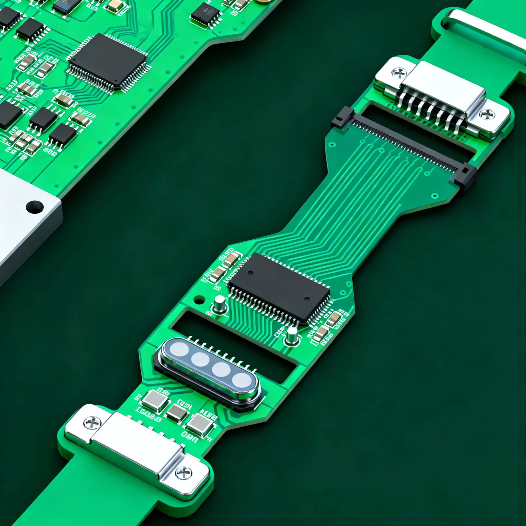
Step-by-Step Rigid-Flex PCB Assembly Tutorial for Smart Wearable Devices
Assembling a rigid-flex PCB for a fitness tracker, smart ring, or continuous glucose monitor is fundamentally different from running a standard rigid board through an SMT line. The polyimide flex laye...
Assembling a rigid-flex PCB for a fitness tracker, smart ring, or continuous glucose monitor is fundamentally different from running a standard rigid board through an SMT line. The polyimide flex layers that make three-dimensional packaging possible also introduce warping risks, stencil printing challenges, and inspection blind spots that most assembly shops never encounter on FR-4-only jobs. At NovaPCBA, we have seen engineering teams arrive with brilliant wearable designs that fail at first article simply because the assembly workflow was not adapted to the hybrid nature of the board. This tutorial walks through the entire process—from panelization strategy through final inspection—with the specific constraints of smart wearable devices in mind.
Why Smart Wearable Devices Are Pushing the Limits of Rigid-Flex Assembly
Smartwatches, medical patches, and fitness trackers demand extreme miniaturization and mechanical reliability that only rigid-flex can deliver. The internal volume of a wearable device is unforgiving: a smart ring may have less than 3 mm of vertical clearance, and even a full-featured smartwatch must fit processors, batteries, sensors, and antennas into a sub-10 mm envelope. As noted in the KingsunPCB 2026 guide, rigid-flex technology enables miniaturization, improved reliability, and user comfort—all essential for next-generation wearable innovation. What makes assembly uniquely challenging is that the same board must survive both the 250°C peak temperatures of lead-free reflow and the 100,000+ dynamic flex cycles the device will experience on a user's wrist or body.
For medical wearables, the stakes are even higher. Fast-turn prototypes are critical to meet clinical validation timelines, requiring assembly workflows that maintain signal integrity across bend zones. According to Fast Turn PCBs, rigid-flex designs in medical applications reduce the bulk of connectors and cable assemblies while improving reliability in space-constrained designs. The assembly process must account for the fact that a single delamination event at the rigid-flex transition can render a Class III medical device nonconforming. Field failures in wearables are disproportionately concentrated at mechanical interfaces—the very zones where rigid and flexible sections meet—making assembly process control at these transitions the single most important quality lever.
The economic pressure also shapes assembly strategy. Consumer wearable volumes routinely reach 500,000+ units per SKU, and a 2% yield loss at final test translates to 10,000 scrapped devices. Assembly engineers working on these products do not have the luxury of learning on the production line; the process must be dialed in before the first panel enters the printer. This is why understanding the full workflow, from panelization to reflow profiling, is not optional—it is prerequisite knowledge for anyone shipping a wearable product in 2025 and beyond.
The Rigid-Flex Assembly Workflow: From Panelization to Reflow
A robust assembly process starts with mounting flex panels on rigid carrier pallets (jigs) to prevent warping during SMT, as detailed in JLCPCB's wearable PCB assembly guide. Because thin polyimide (PI) films can warp during processing, flexible PCBs for wearable electronics are typically mounted on these carrier pallets throughout the entire SMT process, especially during reflow soldering. The pallet material—usually FR-4, aluminum, or a high-temperature composite—must match the thermal expansion characteristics of the flex panel closely enough to avoid introducing shear stress at the pallet-to-board interface.
The guide from AllPCB walks through the complete sequence: stencil printing, pick-and-place, reflow profiling, and final inspection, with an emphasis on defect prevention. What distinguishes rigid-flex assembly from standard rigid PCB assembly is the need to manage two distinct thermal masses within a single board. The rigid sections—often 0.8 mm to 1.6 mm thick with multiple copper layers—absorb heat differently than the 0.1 mm to 0.2 mm flex layers. A reflow profile that brings the rigid section to proper liquidus temperature may overheat the flex area, causing delamination or excessive warping.
The hybrid nature of rigid-flex—uniting rigid and flexible circuit components into one integrated assembly—is explained by FS Circuits, which outlines the unique handling required at each step. Unlike a rigid board that can be handled with standard edge conveyors, a rigid-flex panel must be supported across its entire underside during printing and placement. Any unsupported flex span exceeding 50 mm risks sagging under its own weight, which shifts the stencil-to-board alignment and creates solder paste registration errors that compound through the rest of the line.
Tip: Before committing to a production panelization layout, run a thermal simulation of the full panel—including the carrier pallet—to identify hot spots and cold spots. The cost of simulation is trivial compared to the cost of discovering a 15°C delta across the flex zone during first article.
Process Parameters for Rigid-Flex Wearable Assembly
| Process Step | Parameter | Recommended Value / Range | Notes for Wearable Rigid-Flex |
|---|---|---|---|
| Panel Mounting | Carrier pallet material | FR-4 or aluminum (CTE-matched) | Use high-temperature adhesive tape or mechanical clamps at rigid-only zones; avoid clamping flex areas |
| Stencil Printing | Stencil thickness | 0.08–0.10 mm (flex), 0.12–0.15 mm (rigid) | Step stencil required for mixed rigid-flex; nano-coating recommended for fine-pitch apertures |
| Stencil Printing | Solder paste type | Type 4 or Type 5, no-clean | Type 5 powder for 0201 and 0.4 mm pitch BGAs common in wearables |
| Pick-and-Place | Placement force | 1.5–3.0 N (flex), 2.0–4.0 N (rigid) | Reduce force on flex sections to prevent board deflection; use vacuum nozzle with compliant tip |
| Reflow | Peak temperature | 235–245°C (SAC305) | Profile flex and rigid zones separately with thermocouples; delta T across board <10°C |
| Reflow | Time above liquidus (TAL) | 45–75 seconds | Shorter TAL on flex sections reduces polyimide degradation risk |
| Reflow | Ramp rate | 1.5–2.5°C/second | Gradual ramp prevents thermal shock to adhesive layers at rigid-flex transition |
| Cleaning | Method | No-clean process preferred | Avoid aqueous cleaning on assembled rigid-flex; trapped moisture causes delamination during subsequent reflow or operation |
| Inspection | AOI + X-ray | 100% of rigid zones; selective X-ray on BGA/QFN | Visual inspection under 10× magnification for flex bend areas and transition zones |
| Singulation | Method | Laser routing or precision die cutting | Mechanical routing can fray polyimide edges; laser cutting produces clean edges with minimal stress |
The process parameters above are not starting points—they are the result of iterating through dozens of first-article builds. The most common mistake we see at NovaPCBA is teams treating the rigid-flex board as if it were a rigid board with some thin sections attached. In reality, the flex zones dominate the thermal and mechanical behavior of the entire assembly. If your reflow profile was developed on a rigid-only test vehicle, you are starting from the wrong baseline. The rigid-flex board needs its own profile, developed with thermocouples attached to both the thickest rigid section and the thinnest flex section simultaneously.
Rigid-Flex vs. Hybrid Rigid-FPC Assemblies: When to Eliminate Connectors
Engineers often choose between a single integrated rigid-flex PCB and a rigid board with separate FPC cables joined through ZIF or LIF connectors. PCBMASTER compares smartwatch internal layouts, showing that integrated rigid-flex reduces connector count, improves signal quality, and enhances bend reliability. The elimination of connectors is not merely a component count reduction—it removes an entire failure class. ZIF connectors in wearable devices are notorious for intermittent opens caused by actuator wear, contamination ingress, and micro-fretting corrosion on the contact surfaces.
The KingsunPCB analysis highlights that for wearables under 10 mm thickness, rigid-flex consistently outperforms connector-based assemblies in shock and vibration resistance. A smartwatch dropped from 1.5 meters onto a hard surface experiences peak accelerations exceeding 500g at the board level. A ZIF connector under that load can momentarily separate, causing a system reset or data corruption. A properly designed rigid-flex transition, by contrast, distributes the mechanical stress across a continuous copper layer, eliminating the single-point failure mode.
However, the choice is not always clear-cut. Connector-based architectures offer advantages in repairability, module-level testing, and supply chain flexibility. If a rigid-flex board fails at final test, the entire assembly—including expensive rigid sections—is scrapped. A connectorized design allows the FPC and rigid board to be tested and replaced independently. For low-volume medical devices where field serviceability is a regulatory requirement, the ability to swap a damaged flex section without replacing the entire board can be decisive.
Architecture Comparison: Integrated Rigid-Flex vs. Connectorized FPC
| Comparison Metric | Integrated Rigid-Flex | Rigid Board + Connectorized FPC | Selection Criteria & Failure Boundary |
|---|---|---|---|
| Z-height | As low as 3.5 mm total stack | Typically 6–8 mm minimum (connector adds 2–3 mm) | Choose rigid-flex when total device thickness is below 8 mm; connector height becomes the limiting factor |
| Signal integrity at transition | Continuous copper; no impedance discontinuity | Connector introduces 0.5–1.5 dB insertion loss and potential reflection | Critical for RF traces (Bluetooth, Wi-Fi, UWB) and high-speed digital (MIPI, USB 3.x) |
| Bend cycle reliability | 100k–1M+ cycles with proper design | Connector rated for 10–50 insertion cycles; not designed for dynamic flex | Integrated rigid-flex required for dynamic flex applications; connectorized FPC acceptable for static (fold-once) installations |
| Assembly cost (per unit) | Higher board cost; lower assembly labor | Lower board cost; higher assembly labor (connector placement + FPC insertion) | Rigid-flex becomes cost-competitive above 10k units when assembly labor savings outweigh board cost premium |
| Rework and field service | Full board replacement required | FPC and rigid board independently replaceable | Connectorized preferred for medical devices requiring field serviceability; rigid-flex acceptable for sealed consumer devices |
| Shock/vibration resistance | Excellent; no connector to dislodge | Moderate; connector can momentarily open under >500g shock | Rigid-flex mandatory for sports wearables, military, and high-reliability applications |
| Prototype lead time | 10–15 working days typical | 5–7 working days (standard rigid + off-the-shelf FPC) | Connectorized faster for initial proof-of-concept; transition to rigid-flex for pre-production and production |
The connector-or-rigid-flex decision is fundamentally a trade-off between upfront design complexity and long-term reliability. Engineers who choose rigid-flex are betting that the additional design effort—layer stack-up optimization, bend radius validation, and assembly process development—will pay back through reduced field failures and a more compact product. Those who choose connectorized architectures are prioritizing speed to market and supply chain flexibility. Neither choice is universally correct; the right answer depends on the specific device constraints and the consequences of a field failure.
Design Pitfalls That Sabotage Wearable Rigid-Flex Assembly Yield
Thin polyimide films can warp during reflow if not properly supported. JLCPCB recommends dedicated carrier pallets throughout the entire SMT line—not just during reflow, but from the moment the panel enters the stencil printer until it exits the final inspection station. The pallet is not a convenience; it is a process requirement. We have seen assembly runs where the pallet was removed after placement to speed up reflow cycle time, resulting in a 30%+ warpage-induced defect rate on the flex sections. The few minutes saved were dwarfed by the cost of rework and scrap.
AllPCB's step-by-step guide warns against insufficient pad-to-mask clearances on flex areas and stresses the need for teardrop-shaped vias to prevent stress fractures. The pad-to-mask clearance issue is subtle but consequential: as the flex layer bends, the solder mask—which is more brittle than the polyimide substrate—can crack and propagate into the copper pad. A minimum 75 µm clearance between the pad edge and the solder mask opening is recommended for flex zones, compared to the 50 µm commonly used on rigid boards. Teardrop vias, where the annular ring is widened at the junction with the trace, distribute bending stress across a larger area and reduce the risk of trace cracking at the via shoulder.
Fast Turn PCBs advises that bend radius, layer stack-up symmetry, and selective stiffener placement critically affect assembly stability and long-term reliability. The minimum bend radius rule—typically 10× the flex layer thickness for dynamic applications—is well known, but what is less appreciated is that the bend radius during assembly handling is often tighter than the operational bend radius. A panel that flexes 5 mm as it transitions from the placement machine conveyor to the reflow oven may experience a bend radius of 3–4 mm, well below the design minimum. This is why carrier pallets must extend beyond the panel edges: they prevent handling-induced flex that the designer never intended.
Key Takeaway: The assembly process itself imposes mechanical loads on the flex sections that are separate from—and often more severe than—the operational loads. Design for assembly means designing the flex zones to survive the SMT line, not just the end user's wrist.
Common Yield Killers and Corrective Actions
| Pitfall | Root Cause | Symptom in Assembly | Corrective Action |
|---|---|---|---|
| Flex warping during reflow | Unsupported flex span; CTE mismatch between PI and copper | Open joints, solder bridges, tombstoned passives | Use carrier pallet with full underside support; limit unsupported flex span to <30 mm |
| Delamination at rigid-flex transition | Excessive reflow temperature or TAL at the adhesive layer | Blistering, discoloration, visible separation | Reduce peak temperature at transition zone by 5–8°C; verify adhesive Tg rating exceeds peak reflow temp |
| Trace cracking at via shoulder | Stress concentration at right-angle via-to-trace junction | Intermittent opens, high-resistance traces after bend cycling | Use teardrop vias; increase annular ring to 0.15 mm minimum; avoid 90° trace routing near vias |
| Solder wicking into flex vias | Capillary action draws solder up through via barrel | Reduced flexibility at via location; premature fatigue failure | Specify filled and capped vias in flex areas; use tented vias with 0.05 mm minimum cover |
| Stencil misregistration on flex | Flex section shifts during printing; pallet not flat | Solder paste smearing, insufficient paste on fine-pitch pads | Verify pallet flatness within 0.05 mm across entire surface; use vacuum hold-down during printing |
| Incomplete solder wetting on flex pads | Flex pads oxidize faster than rigid pads; longer storage exposure | Grainy joints, poor wetting, visible de-wetting | Use immersion gold or ENIG finish on flex pads; limit bare board storage to <30 days before assembly |
| Stiffener misalignment | Manual placement of polyimide or FR-4 stiffeners | Bend point shifted; stiffener overlaps component keep-out zone | Specify stiffener placement in CAD with fiducials; use automated pick-and-place for stiffeners where possible |
Beyond these specific pitfalls, there is a broader lesson: rigid-flex assembly yield is a function of upstream design decisions. The assembly team cannot compensate for a poorly designed stack-up, an inadequate bend radius, or a missing stiffener. The most successful wearable programs we support at NovaPCBA are those where the PCB designer and the assembly process engineer collaborate during the layout phase, not after the Gerber files are frozen. A 30-minute design review focused on assembly concerns can prevent weeks of yield debugging.
What Senior Engineers Ask About Rigid-Flex Assembly for Wearables
Q: How do we prevent polyimide flex layers from warping during SMT reflow?
Mount flex panels on rigid carrier pallets (jigs) before stencil printing and keep them on the pallets through placement and reflow. The pallet must provide continuous support under all flex areas—any gap between the pallet and the flex surface creates a zone where the polyimide can sag or curl. Use a controlled reflow profile with a gradual ramp rate of 1.5–2.5°C/second that avoids thermal shock, and consider selective stiffeners (typically 0.1–0.2 mm polyimide or FR-4) to limit unsupported span to less than 30 mm. The adhesive used to bond the flex panel to the pallet must survive peak reflow temperatures without outgassing, which can contaminate solder joints. High-temperature silicone adhesive tapes rated for 260°C+ are commonly used.
Q: What are the critical differences in solder paste stencil design for rigid-flex vs. standard rigid PCBs?
Flex sections often require thinner stencils—0.08 mm to 0.10 mm—to match reduced copper thickness (typically 18 µm or 35 µm on flex layers versus 35 µm to 70 µm on rigid layers). The rigid areas, however, may need thicker paste deposition for larger components like power inductors, connectors, or shield cans, necessitating a step stencil. The step transition must be located on a rigid section, never on or near the flex zone. Aperture walls must be well-defined with a smooth finish; electroformed or nano-coated stencils are preferred for wearable designs with 0.4 mm pitch BGAs or 0201 passives. Account for slight z-axis movement of the flex section during printing—the squeegee pressure can deflect an unsupported flex area by 50–100 µm, altering the effective stencil-to-board gap.
Q: How do you validate dynamic bend reliability for a wearable that will flex thousands of times?
Perform IPC-2223-based cyclic bend testing with real-time resistance monitoring. The test setup should simulate the worst-case bend radius (typically the minimum specified in the design, e.g., 5 mm for a smartwatch flex tail) and the expected number of flex cycles over the product lifetime. For consumer wearables, target a minimum of 100,000 cycles; for medical devices that may be worn continuously for years, 1,000,000+ cycles is appropriate. Monitor resistance change on representative traces—an increase of more than 10% indicates copper fatigue and impending failure. Follow up with cross-section analysis at the bend apex to check for copper cracking, delamination between the copper and polyimide, and adhesive layer degradation. Testing should be performed on assembled boards, not bare flex coupons, because the soldering process can alter the mechanical properties of the flex material.
Q: When should we choose a full rigid-flex design over a rigid board with ZIF/LIF connectors?
Opt for rigid-flex when the total device thickness is below 8 mm, signal integrity at the rigid-to-flex transition is critical (e.g., RF traces for Bluetooth or Wi-Fi, or high-speed MIPI display interfaces), or the device must survive repetitive drops and vibration. Integrated rigid-flex eliminates the connector as a single point of failure—this matters when a field return costs more than the connector itself. If the flex zone is static (folded once during assembly and never moved again) and design volumes are low (under 1,000 units), a connectorized FPC may reduce assembly cost and simplify rework. The breakeven point depends on labor costs, but for most wearable programs exceeding 10,000 units, the assembly labor savings from eliminating connector placement and FPC insertion offset the higher rigid-flex board cost.
Q: What are the most common assembly defects in rigid-flex wearables, and how are they caught?
Typical defects include solder bridging on fine-pitch flex connectors (often driven by excess paste volume or stencil misregistration), cold joints due to uneven thermal mass between rigid and flex sections, and delamination at the rigid-flex transition. Automated optical inspection (AOI) is essential for catching bridging, insufficient solder, and component misalignment on the rigid sections. X-ray inspection is required for BGAs, QFNs, and any component with hidden solder joints. The flex bend areas and the rigid-flex transition zones require visual inspection under 10× to 20× magnification—AOI systems are not typically configured to inspect non-planar surfaces. Look for discoloration (indicating overheating), blistering (delamination), and cracks at the edge of the rigid-flex interface. For high-reliability medical wearables, add cross-section analysis on a sample basis to verify the integrity of the plated through-holes at the transition zone.
Q: How does fast-turn prototyping work for rigid-flex wearable PCBs?
Dedicated quick-turn services, such as those outlined by Fast Turn PCBs, can deliver 5–10 day prototypes by using pre-qualified stack-ups and standard no-clean assembly processes. The key to fast turnaround is avoiding custom materials: use a standard polyimide flex core (e.g., DuPont Pyralux AP or equivalent), standard FR-4 rigid layers, and a pre-qualified adhesive system for the rigid-flex bond. Expect longer lead times—typically 15–20 working days—if the design requires non-standard stiffeners (e.g., stainless steel for spring contacts), controlled impedance on flex layers (which requires tighter process control on dielectric thickness), or exotic materials like liquid crystal polymer (LCP) for high-frequency flex sections. For the fastest prototype cycle, provide the fabricator with a complete stack-up drawing, a detailed bend area definition, and a clear stiffener placement diagram. Ambiguity in any of these areas adds days to the quoting and engineering review process.
At NovaPCBA, we support rigid-flex prototyping with dedicated engineering resources for wearable customers. Our assembly line is configured with carrier pallet fixturing, step stencil capability, and multi-zone reflow profiling specifically for rigid-flex wearable boards. Whether you need five prototypes for a clinical trial or 50,000 units for a consumer launch, the process fundamentals remain the same—but the prototyping phase is where the assembly recipe is developed and validated. Investing in a thorough first-article process pays back in production yield.
References & Further Reading
- PCB Assembly for Wearable Devices: Tips, Materials, and More — JLCPCB
- Mastering Rigid-Flex PCB Assembly: A Step-by-Step Guide for Engineers — AllPCB
- Rigid-Flex PCB Solutions for Smart Wearable Devices (2026 Guide) — KingsunPCB
- Ultimate Guide to Wearable PCB and Design Tips — FS Circuits
- Rigid-Flex PCB For Wearable Medical Devices: Fast-Turn Prototype And Assembly Guide — Fast Turn PCBs
- Rigid-Flex PCBs in Wearables: Advanced Design Challenges and Practical Solutions — PCBMASTER
- NovaPCBA — Rigid-Flex PCB Assembly Services for Smart Wearable Devices
Rigid-flex assembly for wearables is a discipline that rewards process discipline. The engineers who achieve the highest yields are not the ones with the most expensive equipment—they are the ones who understand the thermal and mechanical behavior of the hybrid board at every step of the SMT line. From carrier pallet selection to reflow profiling to bend validation, each decision compounds. When the process is right, a rigid-flex wearable board emerges from the line as a single, reliable, three-dimensional circuit—ready to survive years of flexing on a user's body without a single intermittent connection.