Step-by-Step PCB Assembly Failure Analysis: Techniques to Diagnose and Prevent Issues
Step-by-Step PCB Assembly Failure Analysis: Techniques to Diagnose and Prevent Issues Introduction Printed Circuit Boards (PCBs) are the backbone of modern electronics, serving as the foundation for m...
Introduction
Printed Circuit Boards (PCBs) are the backbone of modern electronics, serving as the foundation for most electronic devices. As technology advances, the complexity of PCBs grows, necessitating more rigorous design and manufacturing processes. With this complexity comes an increased risk of assembly failures, which can lead to costly rework, delays, and compromised product quality. Understanding the intricacies of PCB design, layout rules, stackup design, signal integrity, and manufacturing considerations is crucial for minimizing these risks and ensuring reliable and efficient PCB assembly.
Technical Overview
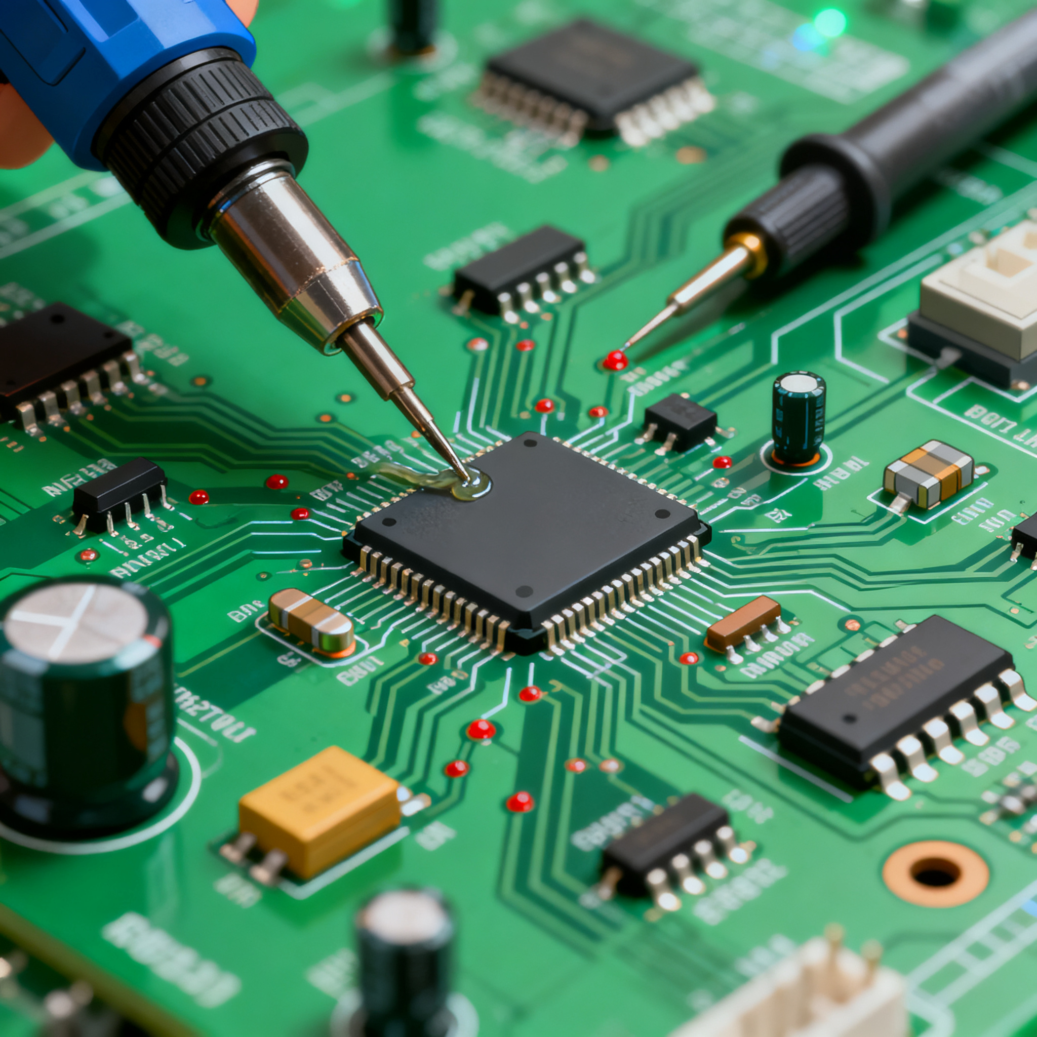
PCB assembly involves the meticulous process of soldering components onto a PCB, which has been designed to meet specific electrical and mechanical requirements. Core concepts include trace routing, via placement, and component footprint design. The architecture of a PCB can range from simple single-layer designs to complex multi-layer configurations, each serving different applications and performance requirements. Principles such as signal integrity and thermal management play a vital role in ensuring the functionality and longevity of the PCB. Adhering to industry standards, such as those set by IPC, can significantly enhance the quality and reliability of PCB assemblies.
Detailed Specifications
In the realm of PCB design, several specifications are critical to ensuring a successful assembly process. These include trace width, spacing, via sizes, and clearances, which directly impact the electrical performance and manufacturability of the PCB. Understanding these parameters is essential for both designers and manufacturers to prevent failure and optimize performance.
| Design Rule | Minimum Value | Recommended Value |
|---|---|---|
| Trace Width | 4 mils | 6 mils |
| Trace Spacing | 4 mils | 8 mils |
| Via Size | 10 mils | 12 mils |
| Pad Size | 20 mils | 24 mils |
| Drill Hole | 8 mils | 10 mils |
| Clearance from Edge | 5 mils | 10 mils |
| Silkscreen Clearance | 4 mils | 6 mils |
| Solder Mask Clearance | 3 mils | 5 mils |
| Component Clearance | 10 mils | 20 mils |
| Aspect Ratio | 6:1 | 8:1 |
Key Takeaways from the Specifications
The specifications outlined in the table are critical for ensuring the manufacturability and reliability of a PCB. Trace width and spacing are particularly important for maintaining signal integrity and preventing cross-talk between adjacent traces. Via sizes and pad sizes must be carefully considered to ensure robust connections and mechanical stability. Clearances, both from the edge and between components, help prevent short circuits and facilitate easier assembly. By adhering to these design rules, engineers can effectively minimize the risk of assembly failures and enhance the overall performance of the PCB.
| Layer Configuration | Signal Layers | Power/Ground Planes |
|---|---|---|
| 2-layer | 2 | 0 |
| 4-layer | 2 | 2 |
| 6-layer | 4 | 2 |
| 8-layer | 4 | 4 |
| 10-layer | 6 | 4 |
| 12-layer | 8 | 4 |
| 14-layer | 10 | 4 |
Practical Implications
The choice of layer stackup significantly impacts the electrical performance and cost of a PCB. A 2-layer board is typically used for simple designs with minimal signal routing requirements. As the complexity of the circuit increases, additional layers are added to accommodate more signal routing and power distribution. The use of dedicated power and ground planes in multi-layer boards helps reduce electromagnetic interference and improve signal integrity. By selecting the appropriate stackup configuration, designers can optimize the PCB for its intended application while balancing cost and performance.
| Material | Dielectric Constant (Dk) | Loss Tangent (Df) |
|---|---|---|
| FR-4 | 4.5 | 0.020 |
| Rogers 4350B | 3.48 | 0.0037 |
| Rogers 4003C | 3.55 | 0.0027 |
| Isola FR408 | 3.75 | 0.015 |
| Nelco N4000-13 | 3.5 | 0.010 |
| Arlon 85N | 3.5 | 0.004 |
| Taconic TLY | 2.2 | 0.0019 |
| Megtron 6 | 3.6 | 0.003 |
| DuPont Pyralux | 3.4 | 0.004 |
Application Guidelines
Selecting the right material for a PCB is crucial for ensuring signal integrity and minimizing losses. Materials like FR-4 are widely used due to their cost-effectiveness and adequate performance for general applications. However, for high-frequency applications, materials with lower dielectric constants and loss tangents, such as Rogers and Taconic, are preferred to reduce signal attenuation. The choice of material should be guided by the specific performance requirements of the application, including frequency, thermal stability, and mechanical properties. By carefully evaluating these factors, engineers can select the most appropriate material to achieve optimal performance and reliability.
Design Considerations
Designing a PCB involves a balance of multiple factors, including electrical, thermal, and mechanical considerations. Signal integrity is paramount, requiring careful attention to trace impedance, length matching, and termination strategies. Thermal management is another critical aspect, particularly for high-power applications, where efficient heat dissipation must be ensured to prevent overheating. Component placement should facilitate easy routing and minimize the length of critical signal paths. Additionally, designers must consider manufacturability, ensuring that the design complies with the capabilities of the chosen PCB manufacturer. This includes adhering to design rules for trace widths, clearances, and via sizes, as well as considering the assembly process and potential rework. By addressing these considerations, engineers can create robust, reliable PCBs that meet the demands of their intended applications.
Step-by-Step Implementation
- Define Requirements: Begin by clearly defining the electrical, mechanical, and environmental requirements of the PCB. This includes power levels, signal frequencies, and any specific form factor constraints.
- Schematic Design: Develop a schematic that accurately represents the circuit, ensuring that all components are correctly specified and interconnected.
- Component Placement: Place components on the PCB layout, prioritizing critical components that influence signal integrity and thermal performance. Ensure that placement facilitates efficient routing and minimizes the length of critical traces.
- Routing: Route traces according to design rules, paying particular attention to impedance control, differential pair routing, and minimizing loop areas to reduce electromagnetic interference.
- Layer Stackup Design: Select an appropriate layer stackup that meets signal integrity and power distribution requirements. Consider the use of dedicated power and ground planes to improve performance.
- Design Rule Check (DRC): Perform a thorough DRC to identify any violations of design rules, such as trace width, spacing, and clearance issues. Resolve any errors before proceeding.
- Prototype and Test: Manufacture a prototype of the PCB and conduct comprehensive testing to validate performance against the defined requirements. Identify and address any issues discovered during testing.
- Finalize Design: Incorporate any necessary changes based on prototype testing and finalize the PCB design for mass production, ensuring that all documentation is complete and accurate.
Common Issues & Solutions
- Open Circuits: Often caused by incomplete solder joints or broken traces. Solution: Inspect solder joints and repair any faulty connections.
- Short Circuits: Result from solder bridges or incorrect component placement. Solution: Use a multimeter to locate shorts and remove excess solder or reposition components.
- Signal Integrity Problems: Caused by improper trace routing or impedance mismatches. Solution: Review and adjust trace routing, ensuring proper impedance control and termination.
- Thermal Issues: Overheating components due to insufficient heat dissipation. Solution: Implement thermal vias, heat sinks, or fans to improve thermal management.
- Component Damage: Due to incorrect soldering temperatures or ESD. Solution: Follow proper soldering guidelines and use ESD protection measures during assembly.
- Manufacturing Defects: Such as misaligned layers or poor solder mask application. Solution: Work closely with the PCB manufacturer to ensure adherence to quality standards and inspect the boards thoroughly before assembly.
Applications & Use Cases
PCBs are integral to a wide range of applications, from consumer electronics to industrial and automotive systems. In consumer electronics, PCBs are used in smartphones, laptops, and wearable devices, where compact size and high performance are critical. In industrial settings, PCBs are used in control systems and instrumentation, requiring robust designs to withstand harsh environments. Automotive applications demand high reliability and thermal performance, particularly in engine control units and infotainment systems. Each application presents unique challenges and requirements, making it essential for engineers to tailor PCB designs to meet specific use case demands.
Selection & Sourcing Guide
When selecting and sourcing components for PCB assembly, it is crucial to consider factors such as availability, cost, and compatibility with the design. Utilizing resources like IC Online can help engineers find the right components quickly and efficiently. Additionally, working with reputable suppliers and manufacturers ensures that the components meet quality standards and are delivered on time. By carefully selecting and sourcing components, engineers can minimize delays and ensure a smooth assembly process.
FAQ
- What is the importance of trace width in PCB design? Trace width affects the current-carrying capacity and resistance of the trace, impacting both electrical performance and thermal management.
- How does layer stackup influence signal integrity? A well-designed stackup can reduce electromagnetic interference and improve signal integrity by providing dedicated power and ground planes.
- What materials are best for high-frequency applications? Materials with low dielectric constants and loss tangents, such as Rogers and Taconic, are preferred for high-frequency applications to minimize signal attenuation.
- How can I prevent thermal issues in my PCB design? Implementing thermal management strategies, such as using heat sinks, thermal vias, and proper layout techniques, can help prevent overheating.
- What are common causes of short circuits in PCB assemblies? Short circuits are often caused by solder bridges, incorrect component placement, or manufacturing defects.
- Why is it important to perform a Design Rule Check (DRC)? A DRC helps identify and resolve potential design rule violations, ensuring that the PCB is manufacturable and meets performance requirements.
- How do I select the right PCB manufacturer? Consider factors such as manufacturing capabilities, quality certifications, lead times, and cost when selecting a PCB manufacturer.
- What role does IPC play in PCB design and manufacturing? IPC standards provide guidelines and best practices for PCB design, assembly, and quality inspection, helping ensure reliability and performance.
- How can I ensure signal integrity in high-speed designs? Proper trace routing, impedance control, and termination strategies are key to maintaining signal integrity in high-speed designs.
- What is the significance of solder mask clearance? Solder mask clearance prevents solder bridging and ensures that solder is applied only to intended areas, reducing the risk of shorts.
Conclusion
PCB assembly failure analysis is a critical aspect of ensuring the reliability and performance of electronic devices. By understanding and applying key design rules, selecting appropriate materials, and considering practical design and manufacturing guidelines, engineers can effectively diagnose and prevent issues. Adopting a systematic approach to PCB design and assembly, supported by industry standards and best practices, will lead to successful outcomes and high-quality products that meet the demands of modern technology.