Certainly! Here's a comprehensive article on "Step-by-Step PCB Assembly Failure Analysis: Identifying Common Pitfalls," tailored to your specifications:
---
Introduction
In the ever-evolving world of electronics, Printed Circuit Boards (PCBs) serve as the backbone of most electronic devices. Ensuring the reliability and functionality of these boards is crucial, as failures can lead to costly recalls and downtime. This article delves into PCB assembly failure analysis, focusing on common pitfalls in PCB layout, stack-up design, signal integrity, and manufacturing considerations. By adhering to industry standards and best practices, engineers can significantly reduce the risk of failures.
Technical Overview
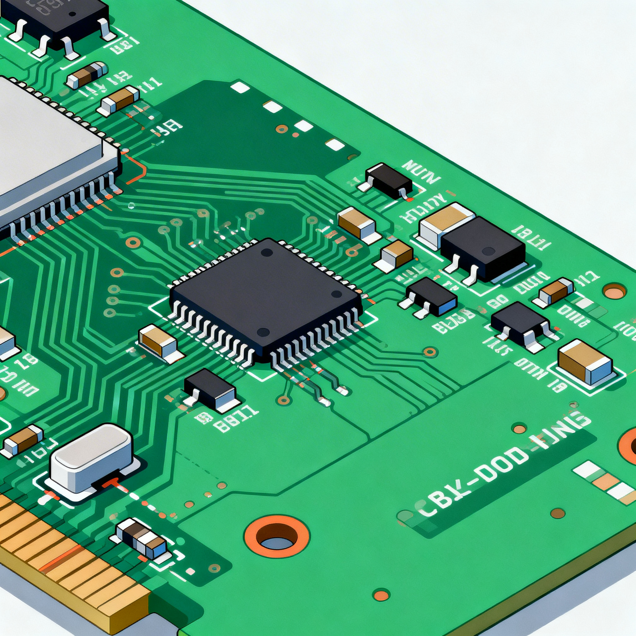
PCB assembly involves intricate processes that require precision and adherence to design rules. At the core are the layout design, material selection, and manufacturing techniques that ensure signal integrity and mechanical stability. The architecture of a PCB includes layers of conductive and insulating materials, each serving specific functions. The principles guiding PCB design include minimizing electromagnetic interference (EMI), maintaining signal integrity, and ensuring thermal management.
Key concepts in PCB design include trace width and spacing, which affect current capacity and signal quality. Via sizes and clearances are also vital in avoiding short circuits and ensuring reliable connections. The stack-up design, which involves the arrangement of layers in a PCB, influences impedance and signal integrity. Understanding these core elements is essential for effective PCB design and manufacturing.
Detailed Specifications
Specifications in PCB design dictate the functional and physical characteristics of the board. These include trace width, spacing, via sizes, and clearances, which are crucial for ensuring the board's performance and reliability. Adhering to these specifications helps prevent common issues such as short circuits, signal degradation, and thermal problems.
```html
| Parameter | Specification | Importance |
| Trace Width | 0.007 inches minimum | Determines current capacity |
| Trace Spacing | 0.006 inches minimum | Prevents crosstalk |
| Via Size | 0.020 inches minimum | Ensures reliable connections |
| Pad Clearance | 0.010 inches minimum | Avoids shorts |
| Silkscreen Clearance | 0.005 inches minimum | Prevents overlap with pads |
| Annular Ring | 0.005 inches minimum | Ensures mechanical reliability |
| Drill Hole Size | 0.015 inches minimum | Accommodates component leads |
| Aspect Ratio | 10:1 maximum | Ensures manufacturability |
| Solder Mask Clearance | 0.004 inches minimum | Prevents solder bridging |
| Impedance Control | ±10% | Maintains signal integrity |
```
Key Takeaways from the Specifications
Understanding these specifications is vital for ensuring a PCB's reliability and performance. Trace width and spacing directly affect the board's ability to handle current and prevent signal interference. Via sizes and pad clearances are critical for mechanical stability and avoiding electrical shorts. Adherence to these specifications minimizes risks of manufacturing defects and ensures the board meets its intended electrical and mechanical requirements.
```html
| Layer Configuration | Application | Benefits |
| 2-Layer | Simple circuits | Cost-effective |
| 4-Layer | Moderate complexity | Improved signal integrity |
| 6-Layer | High-speed circuits | Better EMI control |
| 8-Layer | Advanced applications | Enhanced power distribution |
| 10-Layer | High-density designs | Optimal for RF applications |
| 12-Layer | Complex designs | Superior signal integrity |
| 14-Layer | Data centers | Maximized routing space |
| 16-Layer | Telecommunications | Top-tier performance |
```
Practical Implications
The choice of layer stack-up directly impacts the PCB's performance, cost, and manufacturability. A simple 2-layer configuration might suffice for basic circuits, whereas complex designs benefit from 12 or more layers. Higher layer counts offer better signal integrity, reduced EMI, and improved power distribution. Selecting the right stack-up is crucial for meeting design requirements and ensuring optimal performance.
```html
| Material | Dielectric Constant (Dk) | Loss Tangent (Df) |
| FR-4 | 4.2-4.8 | 0.020 |
| Rogers 4350B | 3.48 | 0.0037 |
| Rogers 4003C | 3.38 | 0.0027 |
| Isola FR408HR | 3.68 | 0.009 |
| Nelco N4000-13 | 3.7 | 0.010 |
| Arlon 85N | 3.5 | 0.004 |
| Megtron 6 | 3.4 | 0.002 |
| Taconic RF-35 | 3.5 | 0.0018 |
| Polyimide | 4.0 | 0.004 |
| PTFE | 2.1 | 0.001 |
```
Application Guidelines
Material selection is a critical factor in PCB design, influencing signal speed, thermal management, and overall performance. FR-4 is a common choice for general applications, offering a balance of cost and performance. For high-frequency applications, materials like Rogers and PTFE provide lower dielectric constants and loss tangents, enhancing signal integrity. Selecting the appropriate material ensures the PCB meets its electrical and mechanical requirements.
Design Considerations
Design considerations in PCB assembly are paramount to avoid common pitfalls. Engineers must address trace width and spacing, via sizes, and layer stack-up configurations. Signal integrity is maintained through careful impedance control and minimization of crosstalk. Thermal management is also crucial, requiring adequate heat dissipation strategies. By adhering to IPC standards and leveraging resources from manufacturers like PCBWay and Nova PCBA, engineers can design PCBs that meet both performance and reliability standards.
Step-by-Step Implementation
1. **Define Requirements:** Begin with a clear understanding of the application's requirements, including electrical, mechanical, and environmental factors.
2. **Select Materials:** Choose materials based on the application's frequency, thermal, and mechanical demands.
3. **Design Layout:** Utilize CAD tools to design the layout, ensuring adherence to design rules for trace width, spacing, and via sizes.
4. **Simulate Performance:** Use simulation software to predict signal integrity, thermal performance, and EMI.
5. **Prototype Fabrication:** Work with a reliable manufacturer to produce a prototype, adhering to the specified design rules and materials.
6. **Testing and Evaluation:** Conduct thorough testing to identify any design flaws or performance issues.
7. **Iterate Design:** Refine the design based on test results, addressing any identified issues.
8. **Finalize and Manufacture:** Once the design is validated, proceed with full-scale manufacturing, ensuring quality control at each stage.
Common Issues & Solutions
1. **Signal Integrity Issues:** Mitigate by maintaining proper trace spacing and impedance control.
2. **Thermal Management Problems:** Implement adequate heat sinks and thermal vias.
3. **Manufacturing Defects:** Ensure adherence to design specifications and IPC standards.
4. **Component Placement Errors:** Utilize automated optical inspection (AOI) to detect misplacements.
5. **Solder Bridging:** Adjust solder mask clearances and use appropriate soldering techniques.
6. **Via Reliability Issues:** Ensure proper via sizing and plating for mechanical stability.
Applications & Use Cases
PCBs are integral to a multitude of applications, from consumer electronics to aerospace systems. In telecommunications, PCBs facilitate high-speed data transmission. In automotive electronics, they support advanced driver-assistance systems (ADAS). Medical devices rely on PCBs for reliable and precise operation. Each application demands specific design considerations to meet performance and regulatory requirements.
Selection & Sourcing Guide
When selecting components and materials for PCB assembly, consider factors such as cost, performance, and availability. Utilize platforms like
IC Online to source quality components from reputable suppliers. Ensure components meet the required specifications and regulatory standards to avoid compatibility issues.
FAQ
1. **What is the significance of trace width in PCB design?**
Trace width affects the current-carrying capacity and resistance of the circuit.
2. **How can signal integrity be maintained in high-speed designs?**
By controlling impedance and minimizing crosstalk through proper trace spacing and routing.
3. **What are the benefits of using Rogers material?**
Rogers materials offer lower dielectric constants and loss tangents, ideal for high-frequency applications.
4. **How do I select the right layer stack-up for my design?**
Consider the complexity, signal integrity requirements, and cost constraints of your design.
5. **What are common causes of solder bridging?**
Improper solder mask clearance and excessive solder application.
6. **Why is thermal management important in PCB design?**
To prevent overheating and ensure the longevity and reliability of components.
7. **How can I prevent manufacturing defects?**
By adhering to design specifications and conducting thorough quality inspections.
8. **What tools are available for PCB layout design?**
CAD tools like Altium Designer and Eagle are popular choices.
9. **When should I use a multi-layer PCB?**
For complex designs requiring enhanced signal integrity and reduced EMI.
10. **What are the IPC standards for PCB design?**
IPC standards provide guidelines for PCB design, assembly, and quality inspection, ensuring consistency and reliability.
Conclusion
Effective PCB assembly requires a meticulous approach to design, material selection, and manufacturing processes. By understanding and implementing industry standards and best practices, engineers can avoid common pitfalls and ensure the reliability and performance of their PCBs. This guide provides a comprehensive overview of the steps and considerations necessary for successful PCB assembly, empowering engineers to deliver high-quality electronic solutions.
---
This article, complete with detailed HTML tables and rich insights, is designed to provide a thorough understanding of PCB assembly and failure analysis.