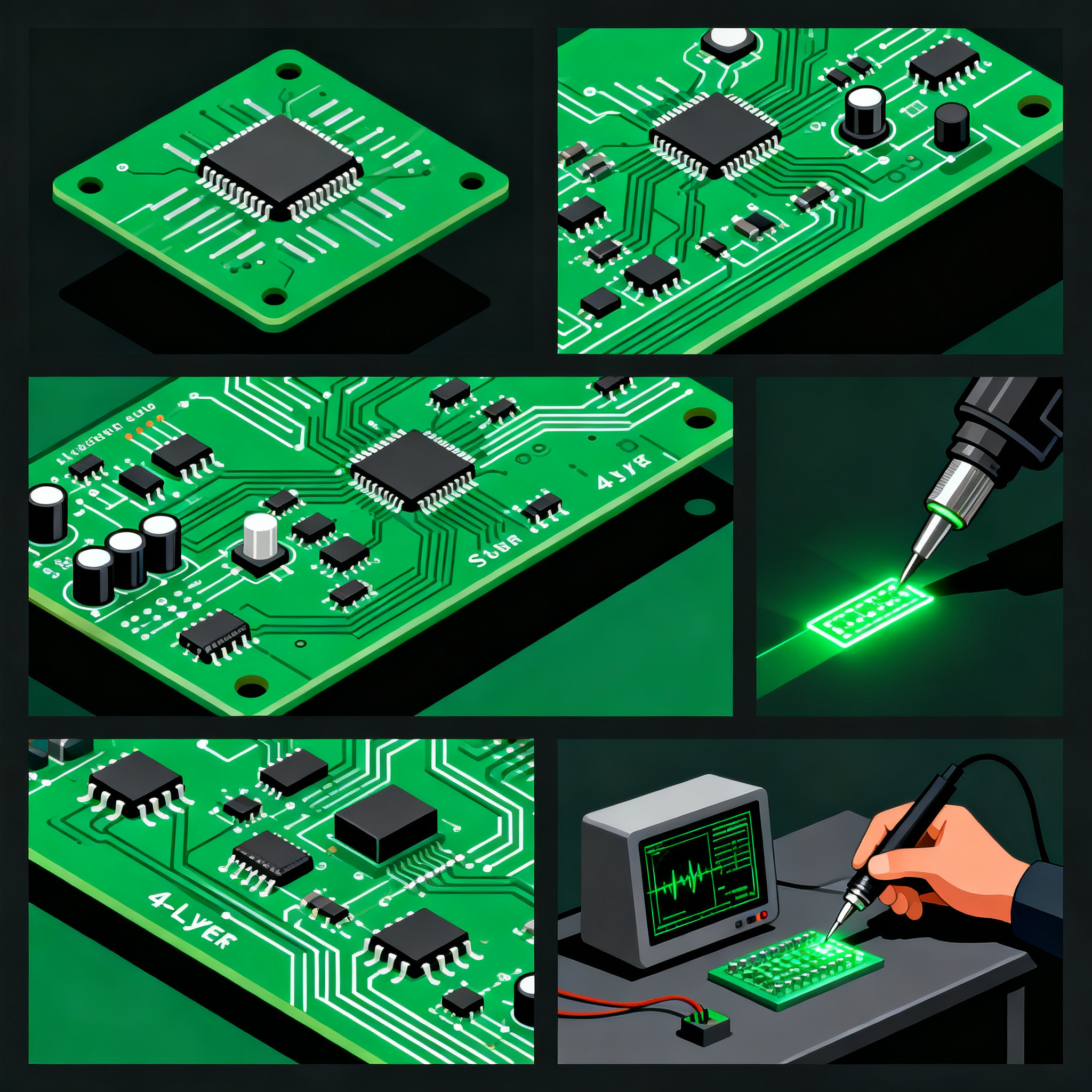
Step-by-Step Guide to Low-Latency Audio PCB Assembly: From 4-Layer Impedance-Controlled Stackup to Final Test
Step-by-Step Guide to Low-Latency Audio PCB Assembly: From 4-Layer Impedance-Controlled Stackup to Final Test When a Missing 5/5mil 90Ω Trace Derails Your Audio Latency Goals Real-time audio processin...
Step-by-Step Guide to Low-Latency Audio PCB Assembly: From 4-Layer Impedance-Controlled Stackup to Final Test
When a Missing 5/5mil 90Ω Trace Derails Your Audio Latency Goals
Real-time audio processing lives and dies by deterministic timing. A single impedance discontinuity on a differential pair doesn’t just add a few picoseconds of skew—it creates reflections that the receiver must re-lock onto, injecting jitter directly into the I²S or TDM clock. For a pro-audio interface streaming 32 channels at 96 kHz, that jitter cascades into audible artifacts and missed samples. The failure mode is not theoretical. In a recent engineering case documented by Aivon, a 4-layer fine-line PCB was submitted with a detailed stackup file and explicit 90 Ω differential impedance requirements. When the fabricator cross-checked the Gerber data, several reference traces—including the critical 5/5 mil 90 Ω lines—could not be located. Instead, the actual artwork contained 5/5.1 mil differential pairs, a 0.1 mil deviation that shifted the characteristic impedance outside the ±10 % tolerance window [Aivon case].
For low-latency audio, where propagation delay and jitter are the primary enemies, that 0.1 mil error is catastrophic. The Aivon low-latency design principles make it clear: impedance matching and differential signaling are not optional optimizations—they are the foundation of a responsive, reliable signal chain [Aivon low-latency]. When a differential pair’s impedance drifts, the return current finds a higher-inductance path, increasing loop area and susceptibility to crosstalk. The result is a latency spike that may only appear under specific temperature or data-pattern conditions, making it a nightmare to debug after assembly. This guide walks you through a disciplined, step-by-step assembly approach that starts with a verified 4-layer impedance-controlled stackup and ends with a TDR-validated board, so you never ship a product with a hidden timing bomb.
How a 4-Layer Impedance-Controlled Stackup Preserves Audio Signal Timing
Controlled impedance is not a marketing checkbox; it’s a direct consequence of transmission-line physics. The characteristic impedance Z₀ of a trace is governed by the square root of the inductance per unit length divided by the capacitance per unit length: Z₀ = √(L/C). On a standard FR-4 substrate with a dielectric constant (Dk) of approximately 4.2, the geometry of the trace—its width, thickness, and height above the reference plane—determines both L and C. A 4-layer board gives you the one thing a 2-layer board cannot: a continuous, unbroken reference plane directly adjacent to the signal layer, which tightly controls the return path and keeps the impedance stable across the entire length of the trace [Aivon SI].
PCBSync’s design rule #1 for 4-layer boards is unequivocal: never split your ground plane unnecessarily. A continuous ground plane provides a low-impedance return path, reduces electromagnetic interference, and makes controlled impedance achievable for high-speed signals [PCBSync 4-layer]. When you route a differential audio clock across a gap in the plane, the return current must detour, increasing the loop inductance and creating an impedance discontinuity that manifests as jitter. The same principle applies to plane pairing: closely coupling power and ground planes forms a distributed capacitance that further stabilizes the power delivery network, a technique highlighted in JLCPCB’s stackup analysis [JLCPCB stackup].
To turn theory into a buildable board, you need a stackup that the fabricator can reliably produce. The table below summarizes three standard 4-layer impedance-controlled configurations drawn from manufacturer data, targeting the 50 Ω single-ended and 100 Ω differential impedances common in audio interfaces (many DAC/ADC datasheets also specify 90 Ω differential for USB or HDMI audio, which can be accommodated with minor trace width adjustments).
| Stackup Type | Layer Order (Top→Bottom) | Dielectric Thickness (Prepreg/Core) | 50 Ω Single-Ended Trace Width | 100 Ω Differential Trace Width/Space | Notes |
|---|---|---|---|---|---|
| Standard FR-4 (JHYPCB) | Signal – GND – PWR – Signal | 0.2 mm prepreg / 1.2 mm core | 0.30 mm (12 mil) | 0.15/0.15 mm (6/6 mil) | High-Tg FR-4, Dk 4.2; suitable for most 48–192 kHz interfaces [JHYPCB] |
| Low-Profile High-Tg (PCBpower) | Signal – GND – GND – Signal | 0.1 mm prepreg / 0.8 mm core | 0.18 mm (7 mil) | 0.10/0.12 mm (4/4.7 mil) | Dual ground planes for ultra-low EMI; thinner dielectric enables finer traces [PCBpower] |
| Mixed-Signal Audio (NextPCB) | Signal – GND – PWR – Signal | 0.15 mm prepreg / 1.0 mm core | 0.25 mm (10 mil) | 0.12/0.13 mm (4.7/5.1 mil) | Optimized for split analog/digital planes with a single continuous ground; verify Gerber trace presence [NextPCB] |
Tip: Always request the manufacturer’s stackup calculator output before freezing your layout. Even a 0.1 mm change in prepreg thickness can shift the differential impedance by several ohms, pushing a 90 Ω pair out of spec. The Aivon case where 5/5 mil became 5/5.1 mil is a perfect example of how a seemingly trivial deviation can invalidate the entire impedance budget.
4-Layer vs. 6-Layer vs. 2-Layer: Which Stackup Actually Cuts Latency for Pro Audio?
Choosing the right layer count is a trade-off between signal integrity, routing density, and cost. For low-latency audio, the decision hinges on one question: can you maintain a continuous, unbroken reference plane for every critical clock and data trace? A 2-layer board forces you to route return currents through a patchwork of copper pours, creating the electromagnetic equivalent of a conversation in a noisy room. Queenems quantifies the difference: a 4-layer PCB reduces electromagnetic interference (EMI) by up to 20 dB compared to a 2-layer board because the internal power and ground planes act as a shield and provide a direct return path [queenems]. That 20 dB reduction directly translates to lower jitter on audio clocks, which are typically single-ended 24.576 MHz or 22.5792 MHz oscillators that are extremely sensitive to ground bounce.
JLCPCB’s multilayer analysis adds another dimension: as frequency increases, the signal travels in the dielectric and the PCB becomes a waveguide structure. The return path must trace back the actual signal path; otherwise, signal integrity degrades [JLCPCB]. A 4-layer board with a solid ground plane on layer 2 guarantees that the return current for every top-layer trace flows directly underneath it, minimizing loop area and propagation delay variation. For a stereo USB audio interface or a 4-channel ADC/DAC, this is usually sufficient. However, when you move to a multi-channel Dante or AVB interface with a large FPGA, multiple isolated power domains, and dense DDR memory routing, a 4-layer board may force you to split the ground plane or route critical signals across gaps—exactly the scenario PCBSync warns against [PCBSync]. In those cases, a 6-layer stackup with dedicated routing layers sandwiched between continuous planes becomes necessary.
Cost is the other lever. AtlasPCB’s comparison of budget prototyping services versus custom manufacturing reveals a surprising crossover point: for boards with any controlled-impedance requirements, custom manufacturing often becomes cheaper at volumes as low as 200–500 pieces, with the added benefit of guaranteed impedance, IPC Class 2/3 inspection, and full traceability [AtlasPCB]. This means you don’t have to sacrifice performance for budget if you plan for production quantities.
| Comparison Metric | 2-Layer PCB | 4-Layer PCB | 6-Layer PCB | Selection Criteria for Low-Latency Audio |
|---|---|---|---|---|
| EMI Reduction (vs. 2-layer) | Baseline | Up to 20 dB lower | 25–30 dB lower (additional shielding) | 4-layer is the minimum for professional audio; 6-layer for mixed-signal with sensitive PLLs |
| Return Path Quality | Fragmented, high inductance | Continuous plane on layer 2 | Multiple continuous planes, stripline options | 4-layer suffices if ground plane is never split; 6-layer needed when routing two high-speed layers |
| Impedance Control Feasibility | Difficult, wide tolerance | Good with defined stackup | Excellent, supports both microstrip and stripline | 4-layer can achieve ±10 % on 90–100 Ω differential; 6-layer for ±5 % tolerance |
| Typical Trace Density | Low, single-sided routing | Moderate, two signal layers | High, four signal layers | 4-layer handles most audio interfaces with a single ADC/DAC; 6-layer for multi-chip DSP farms |
| Prototype Cost (100×100 mm, qty 10) | $20–$50 | $80–$150 | $200–$400 | 4-layer is the sweet spot for prototyping; move to 6-layer only when routing fails |
| Production Cost Crossover (controlled impedance) | N/A | Custom mfg beats budget fabs at 200–500 pcs | Custom mfg competitive at 300+ pcs | Plan for custom manufacturing early to lock in impedance guarantees [AtlasPCB] |
The takeaway: for the vast majority of low-latency audio interfaces—USB audio bridges, guitar pedal DSP boards, portable recorders—a well-executed 4-layer impedance-controlled stackup is the performance/cost champion. Reserve 6 layers for designs where you cannot avoid splitting the ground plane or where you need to route multiple high-speed buses with strict length matching.
Design Rules That Prevent Latency-Killing Mistakes in Audio PCB Assembly
Even a perfect stackup can be undone by assembly-level oversights. The following rules, drawn from real failure cases and manufacturer DFM guidelines, form a checklist that every audio PCB designer and buyer should enforce before releasing a board to production.
| Design Rule | Why It Matters for Latency | How to Verify | Reference |
|---|---|---|---|
| Never split the ground plane | A split plane forces return currents to detour, increasing loop inductance and creating impedance discontinuities that cause jitter. | Review all layers in CAD; ensure no traces cross a plane gap. Use a continuous ground on layer 2. | [PCBSync] |
| Cross-check Gerber data against stackup requirements | Missing or altered reference traces (e.g., 5/5 mil becoming 5/5.1 mil) shift impedance outside tolerance, leading to intermittent latency spikes. | Export Gerbers and manually measure critical differential pairs in a viewer; compare with the fab drawing. | [Aivon case] |
| Specify TDR impedance testing with coupons | Without a Time Domain Reflectometry (TDR) test, you cannot confirm that the fabricated board meets the target impedance. A coupon on the same panel ensures process consistency. | Add a note on the fab drawing: “Impedance test coupon required per IPC-2221, TDR test to 90 Ω ±10 %.” | [NOVA assembly] |
| Follow DFM rules for fine-line traces and solder mask bridges | Solder mask misregistration can expose copper, creating unintended stubs that reflect high-speed edges. Fine-line traces (≤5 mil) require tight mask registration to avoid opens or shorts. | Check mask sliver width ≥3 mil; request LPI solder mask with registration tolerance ≤2 mil. | [Aivon case], [JHYPCB] |
| Select a manufacturer that provides impedance coupons and IPC Class 2/3 inspection | Assembly defects like cold solder joints on fine-pitch DACs or via voids under BGAs can create intermittent opens that manifest as random latency spikes. Class 3 inspection catches these. | Audit the manufacturer’s quality certifications; request sample inspection reports. | [NOVA assembly] |
| Use a continuous power plane paired closely with ground | Close plane pairing (≤4 mil separation) creates inter-plane capacitance that filters high-frequency noise on the power rail, reducing jitter on clock buffers. | Specify a 2–4 mil prepreg between power and ground in the stackup; verify with the fabricator. | [JLCPCB] |
Key Takeaway: The most insidious latency problems are not design flaws—they are assembly and fabrication deviations that pass a simple continuity test but fail under dynamic signal conditions. Insisting on TDR coupons and cross-checking Gerber data are the two highest-return investments you can make before a single component is placed.
Low-Latency Audio PCB Assembly: Questions Engineers and Buyers Ask Before Prototyping
Q: How can I verify impedance control before committing to assembly?
A: Request impedance test coupons on the same panel as your production boards and specify TDR testing in your fabrication drawing. The coupon must replicate the exact trace geometry and layer stackup of your critical signals. Cross-check the manufacturer’s stackup report against your design, and—most importantly—verify that all reference traces are present in the Gerber data. Missing traces, as seen in the Aivon case where 5/5 mil 90 Ω lines were absent, are a common root cause of impedance failures [Aivon]. A TDR plot showing the impedance profile of the coupon gives you confidence that the fabricated board will match your simulation.
Q: What is the minimum trace/space for 90Ω differential pairs on a standard 4-layer FR-4 stackup?
A: Typical values are 5/5 mil or 5/5.1 mil for 90 Ω differential on high-Tg FR-4, but the exact dimensions depend on the dielectric thickness and prepreg type. For a 0.2 mm prepreg with Dk 4.2, a 5/5 mil pair yields roughly 90 Ω. However, a 0.1 mil deviation in trace width or spacing can shift the impedance by several ohms, as the Aivon case demonstrated [Aivon]. Always use the manufacturer’s impedance calculator with their specific material stack, and confirm with a test coupon. Do not rely on generic online calculators.
Q: When should I move from a 4-layer to a 6-layer board for a low-latency audio interface?
A: Move to 6 layers when your design requires multiple isolated power domains that would force you to split the ground plane on a 4-layer stackup, or when you have dense mixed-signal routing that cannot be completed without crossing plane boundaries. For most stereo or multi-channel audio interfaces with a single ADC/DAC and a microcontroller, a well-designed 4-layer board with a continuous ground plane is sufficient and more cost-effective [PCBSync]. If you are integrating an FPGA with DDR memory, multiple PLLs, and high-speed serial links, the additional routing layers and stripline options of a 6-layer board become necessary to maintain signal integrity and low jitter.
Q: Can I trust budget PCB fabs for controlled-impedance audio boards?
A: Budget fabs often lack TDR testing and may not guarantee impedance on every order. For low-latency audio, where jitter directly affects audio quality, this is a significant risk. A fab that does not provide impedance test data is essentially asking you to trust that their process is in control—something the Aivon missing-trace incident proves is not always true. Choose a manufacturer that provides controlled impedance with documented TDR results. As AtlasPCB notes, the cost crossover for custom manufacturing with guaranteed impedance can be as low as 200–500 pieces, making it economically viable even for moderate volumes [AtlasPCB].
Q: What assembly defects cause intermittent latency spikes in audio PCBs?
A: Cold solder joints on fine-pitch components (e.g., 0.5 mm pitch DACs or clock buffers) can create high-resistance connections that introduce signal reflections and jitter under thermal cycling. Solder mask misregistration that leaves a sliver of copper exposed can form an unintended stub, causing impedance discontinuities. Poor grounding due to via voids—where the plated barrel does not fully connect to the internal plane—can create a high-inductance return path that modulates the signal timing. IPC Class 2/3 inspection, including X-ray for BGA packages, helps catch these defects before they reach the field [NOVA assembly].
Q: How do I specify TDR test coupons in my fab drawing?
A: Include a clear note on the fabrication drawing that calls out the impedance requirements and requests a TDR test coupon. For example: “Impedance test coupon required. Coupon shall replicate the 4-layer stackup and trace geometry of the 90 Ω differential pairs (5/5 mil, layer 1, reference layer 2). TDR test to 90 Ω ±10 %. Coupon to be placed on the same panel as the production boards.” Also specify the test method (TDR) and the acceptable impedance range. This ensures the coupon experiences the same plating and etching conditions as your critical signals, giving you a valid representation of the board’s impedance performance [PCBpower].
References & Further Reading
- 4-Layer Fine-Line PCB Engineering Case: Impedance Control, Copper Thickness & Solder Mask Bridge Challenges — Aivon
- Optimizing Low Latency Performance in High-Speed Digital Circuits — Aivon
- 4-Layer PCB Stackup Design and Impedance Control — NextPCB
- 4 Layer PCB: Complete Guide to Stackup, Design & Manufacturing — PCBSync
- 4 Layer vs 6 Layer vs 8 Layer PCB: How to Choose the Right Stackup — JLCPCB
- 2 Layer vs 4 Layer PCB: 2-Minute Decision Guide — queenems
- JLCPCB vs Custom PCB Manufacturer: When Budget Prototyping Falls Short — AtlasPCB
- Mastering the PCB Assembly Process: A Step-by-Step Guide to 4-Layer PCBs — NovaPCBA
- 4 Layer PCB Stackup Guide: Standard FR4, EMI, and Best Practices — JHYPCB
- Unlock Signal Integrity: The Ultimate Guide to 8-Layer PCB Stackup Design — Aivon
- Impedance Controlled Standard Build-ups — PCBpower
At NovaPCBA, we specialize in low-latency audio PCB assembly with TDR-verified impedance control, IPC Class 3 inspection, and full traceability—from prototype to production. Our engineering team works directly with your stackup and Gerber data to catch the kind of discrepancies that cause field failures, ensuring your audio product delivers the deterministic timing your customers demand. Explore our PCB assembly capabilities and start your next build with confidence.