Step-by-Step Guide to Designing Efficient PCBs for Smart Home Device Assembly
Step-by-Step Guide to Designing Efficient PCBs for Smart Home Device Assembly Introduction The rapid evolution of smart home technologies has significantly increased the demand for efficient and relia...
Introduction
The rapid evolution of smart home technologies has significantly increased the demand for efficient and reliable printed circuit boards (PCBs). As the backbone of electronic devices, PCBs play a crucial role in ensuring seamless functionality and integration of various components. This article provides a comprehensive guide to designing efficient PCBs for smart home devices, focusing on component specifications, datasheets, selection criteria, and application circuits. Utilizing industry standards and best practices, electronics engineers can enhance product performance and reliability, meeting the growing consumer expectations in the smart home market.
Technical Overview
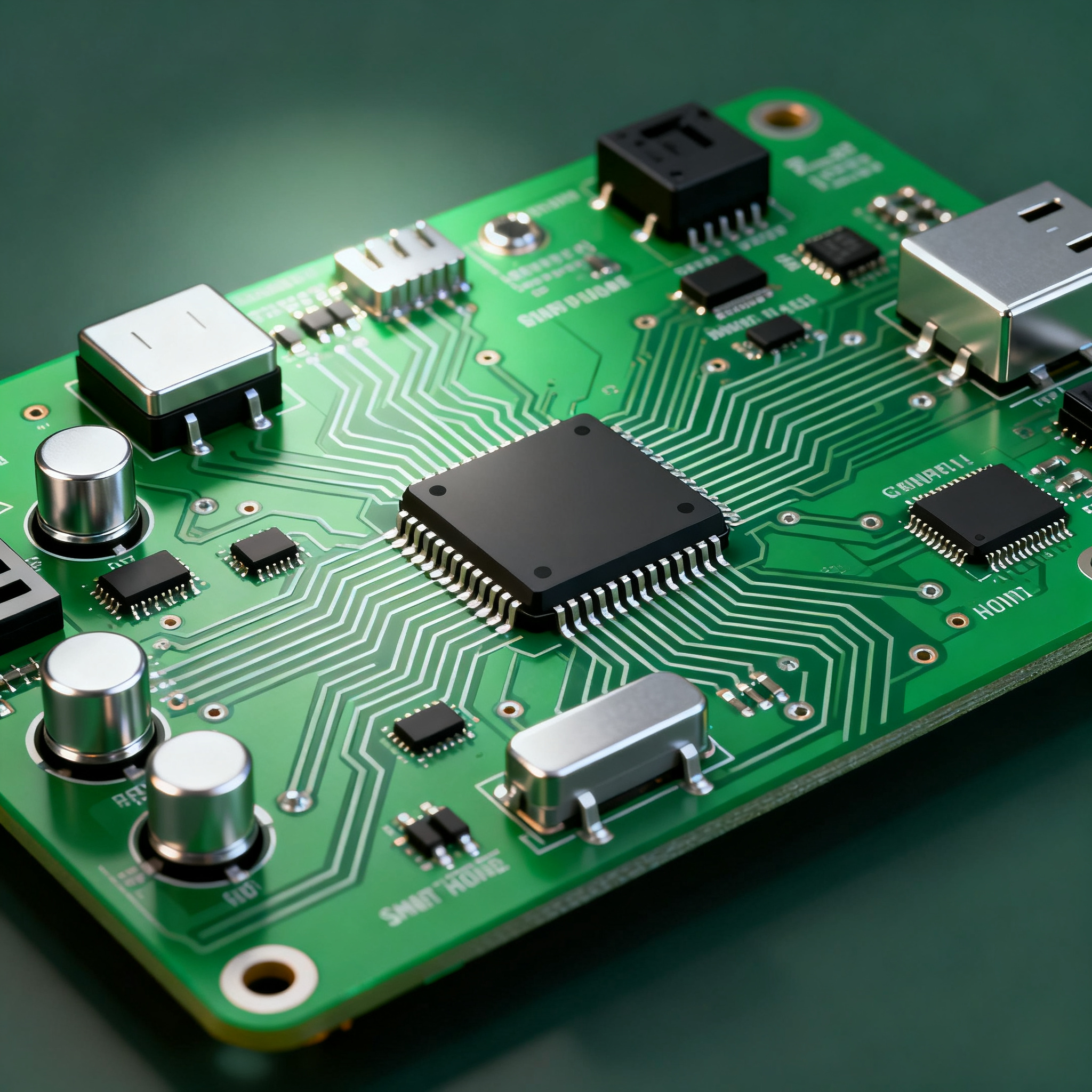
Designing a PCB for smart home devices involves understanding core concepts such as signal integrity, power distribution, and thermal management. The architecture of a PCB is critical, as it dictates how components are interconnected and how signals are routed. Principles such as minimizing electromagnetic interference (EMI) and optimizing trace routing are essential for maintaining signal integrity and ensuring efficient power distribution. Adhering to industry standards like IPC-2221 and IPC-A-610, which provide guidelines for design and quality inspection, can significantly enhance the reliability and manufacturability of PCBs.
Another crucial aspect of PCB design is the selection of appropriate components, which involves reviewing datasheets to understand specifications such as CPU speed, memory, and power requirements. Application circuits must be designed to accommodate these specifications while ensuring compatibility with other components. By leveraging resources from PCB manufacturers and assembly services, engineers can create designs that are not only efficient but also cost-effective and scalable.
Detailed Specifications
Understanding and selecting the correct specifications for IC chips is crucial in PCB design. This includes evaluating CPU speed, memory capabilities, peripheral support, power requirements, and packaging options. These specifications determine the performance and efficiency of the PCB, impacting the overall functionality of the smart home device. Below is a table outlining core specifications for typical IC chips used in smart home devices.
| Specification | Description | Value |
|---|---|---|
| CPU Speed | Processor clock speed | 1.2 GHz |
| Memory | RAM capacity | 512 MB |
| Flash Storage | Non-volatile memory | 4 GB |
| Peripherals | Supported interfaces | UART, SPI, I2C |
| Power Supply | Operating voltage range | 3.3V - 5V |
| Package Type | Physical packaging of IC | LQFP, 64-pin |
| Temperature Range | Operating temperature limits | -40°C to 85°C |
| GPIO | General-purpose I/O pins | 16 pins |
| ADC | Analog-to-digital converters | 10-bit |
| DAC | Digital-to-analog converters | 8-bit |
| Timer/Counters | Number of timers available | 3 |
| Watchdog Timer | System reset timer | Available |
Key Takeaways from the Specifications
The specifications outlined in the table above are critical in determining the suitability of an IC chip for smart home devices. The CPU speed and memory capacity directly impact the processing power and efficiency of the device, making them crucial for applications requiring real-time data processing. The availability of peripherals such as UART, SPI, and I2C ensures compatibility with a wide range of sensors and modules, facilitating seamless integration into smart home networks. Power supply specifications, including operating voltage range, are essential for ensuring reliable operation under varying power conditions. Moreover, the package type and temperature range provide insights into the physical and environmental constraints the device can endure, aiding in the selection of components that meet specific application requirements.
| Characteristic | Description | Value |
|---|---|---|
| Operating Voltage | Minimum and maximum voltage | 3.3V - 5V |
| Operating Current | Typical current consumption | 150 mA |
| Standby Current | Current in standby mode | 1.5 mA |
| Input Voltage Range | Voltage range for inputs | 0V - 5V |
| Output Current | Maximum current for outputs | 20 mA per pin |
| Clock Frequency | Internal clock speed | 16 MHz |
| Propagation Delay | Signal delay time | 10 ns |
| Rise/Fall Time | Time for signal to rise or fall | 5 ns |
| Input Capacitance | Capacitance of input pins | 5 pF |
| Output Capacitance | Capacitance of output pins | 10 pF |
| Thermal Resistance | Thermal resistance junction-to-ambient | 60°C/W |
| ESD Protection | Electrostatic discharge protection level | ±2 kV |
Practical Implications
The electrical characteristics table provides essential data that influences the design and functionality of smart home devices. Operating voltage and current specifications are critical for ensuring the device operates within safe limits, preventing damage due to overvoltage or overheating. Standby current is particularly important for battery-operated devices, as it affects power efficiency and battery life. Propagation delay and rise/fall times are crucial for high-speed applications, impacting signal timing and synchronization. Additionally, thermal resistance and ESD protection are vital for ensuring the device's durability and resilience in various environmental conditions. Understanding these characteristics allows engineers to design circuits that maximize performance while minimizing potential issues.
| Use Case | Configuration | Benefits |
|---|---|---|
| Smart Lighting | Low-power MCU with RF module | Energy-efficient, remote control |
| Security Systems | High-speed MCU with multiple I/O | Real-time monitoring, quick response |
| Thermostats | MCU with ADC and temperature sensors | Precise temperature control, energy savings |
| Smart Plugs | MCU with power monitoring IC | Energy consumption tracking, remote operation |
| Voice Assistants | High-performance MCU with DSP | Efficient voice processing, seamless interaction |
| Home Automation Hub | MCU with extensive connectivity options | Centralized control, integration with multiple devices |
| Smart Appliances | MCU with motor control and sensors | Improved efficiency, smart functionality |
| Environmental Sensors | Low-power MCU with wireless connectivity | Continuous monitoring, remote data access |
Application Guidelines
The application comparison table highlights the versatility of MCU configurations in various smart home devices. For instance, smart lighting systems benefit from low-power MCUs with RF modules, enabling energy-efficient operation and remote control capabilities. Security systems require high-speed MCUs with multiple I/O options for real-time monitoring and quick response. Thermostats utilize MCUs with ADCs and temperature sensors for precise temperature control, enhancing energy savings. Smart plugs leverage power monitoring ICs to track energy consumption, allowing users to manage devices remotely. Each configuration is tailored to specific applications, ensuring optimal performance and user satisfaction. By understanding these applications, engineers can make informed decisions when selecting components and designing circuits.
Design Considerations
When designing PCBs for smart home devices, several key considerations must be taken into account to ensure optimal performance and reliability. Firstly, component placement is critical for minimizing signal interference and optimizing thermal management. Placing components strategically can enhance signal integrity and reduce EMI, leading to improved device performance. Additionally, trace routing should be carefully planned to minimize signal paths and reduce the risk of crosstalk.
Power distribution is another vital aspect, as it directly impacts the efficiency and stability of the device. Implementing robust power distribution networks (PDNs) can help manage voltage drops and ensure consistent power delivery to all components. Thermal management is equally important, as excessive heat can lead to component failure and reduced lifespan. Utilizing heat sinks, thermal vias, and appropriate board materials can aid in effective heat dissipation.
Adhering to industry standards such as IPC-2221 and IPC-A-610 is essential for ensuring manufacturability and quality control. These standards provide guidelines for design, assembly, and inspection, helping engineers create reliable and high-quality PCBs. Collaboration with PCB manufacturers and assembly services can also provide valuable insights and resources, enabling engineers to optimize designs for production and scalability.
Step-by-Step Implementation
- Define Requirements: Begin by identifying the specific requirements of the smart home device, including functionality, performance, and environmental constraints. This step involves understanding the application and determining the necessary components and specifications.
- Component Selection: Review datasheets and specifications to select appropriate components, such as MCUs, sensors, and power management ICs. Ensure compatibility and performance alignment with the device's requirements.
- Create Schematic: Design the circuit schematic using CAD software, incorporating all selected components and ensuring correct connectivity. Pay attention to signal paths and power distribution to optimize performance.
- PCB Layout: Develop the PCB layout, focusing on component placement and trace routing. Consider factors such as signal integrity, thermal management, and manufacturability to create an efficient and reliable design.
- Design Rule Check (DRC): Perform a design rule check to identify and resolve any layout issues. Ensure compliance with industry standards and manufacturer guidelines to facilitate production.
- Prototype and Test: Manufacture a prototype PCB and conduct thorough testing to validate the design. Evaluate performance, functionality, and reliability under various conditions to ensure the device meets specifications.
- Iterate and Optimize: Based on testing results, make necessary adjustments to the design to address any issues or improve performance. Iterate the design process as needed to achieve optimal results.
- Finalize Design: Once the design is validated and optimized, finalize the PCB layout and prepare for mass production. Collaborate with PCB manufacturers and assembly services to ensure a smooth transition to production.
Common Issues & Solutions
- Signal Integrity Problems: Issues such as crosstalk and EMI can degrade signal quality. Solutions include careful trace routing, using ground planes, and implementing shielding techniques.
- Thermal Management Challenges: Excessive heat can lead to component failure. Implementing heat sinks, thermal vias, and selecting materials with good thermal conductivity can help manage heat dissipation.
- Power Distribution Issues: Voltage drops and inconsistent power delivery can affect performance. Designing robust PDNs and using decoupling capacitors can ensure stable power distribution.
- Manufacturing Defects: Errors during fabrication and assembly can lead to defects. Collaborating with experienced manufacturers and adhering to industry standards can minimize the risk of defects.
- Design Rule Violations: Non-compliance with design rules can hinder manufacturability. Regular design rule checks and adherence to guidelines can prevent violations.
- Component Mismatch: Incompatibility between components can cause functionality issues. Thoroughly reviewing datasheets and compatibility before selection can prevent mismatches.
Applications & Use Cases
Smart home devices encompass a wide range of applications, each with unique requirements and configurations. For instance, smart lighting systems often incorporate low-power MCUs and RF modules for energy efficiency and remote control capabilities. Security systems require high-speed MCUs with multiple I/O options for real-time monitoring and quick response. Thermostats utilize MCUs with ADCs and temperature sensors for precise temperature control, enhancing energy savings. Each application demands specific design considerations and component selections to achieve optimal performance and functionality.
Selection & Sourcing Guide
When selecting and sourcing components for PCB design, it is essential to consider factors such as availability, cost, and compatibility. Utilizing online resources such as IC Online can aid in identifying suitable components and suppliers. Additionally, collaborating with manufacturers and assembly services can provide valuable insights and resources for optimizing designs and ensuring a smooth production process.
FAQ
- What are the key considerations when designing PCBs for smart home devices? Key considerations include component placement, trace routing, power distribution, thermal management, and adherence to industry standards.
- How can I ensure signal integrity in my PCB design? Signal integrity can be ensured by careful trace routing, using ground planes, and implementing shielding techniques to minimize crosstalk and EMI.
- What is the importance of thermal management in PCB design? Effective thermal management prevents overheating, which can lead to component failure and reduced lifespan. Implementing heat sinks, thermal vias, and selecting appropriate materials is crucial.
- How do I select the right components for my PCB design? Review datasheets and specifications to ensure compatibility and performance alignment with the device's requirements. Consider factors such as availability, cost, and compatibility.
- What are common issues faced during PCB manufacturing? Common issues include signal integrity problems, thermal management challenges, power distribution issues, manufacturing defects, and design rule violations.
- How can I address manufacturing defects in my PCB design? Collaborating with experienced manufacturers and adhering to industry standards can minimize the risk of defects during fabrication and assembly.
- Why is power distribution important in PCB design? Power distribution directly impacts the efficiency and stability of the device. Designing robust PDNs and using decoupling capacitors can ensure stable power delivery.
- What resources are available for PCB design and manufacturing? Resources such as IPC standards, PCBWay, and Nova PCBA provide valuable guidelines, design rules, and manufacturing capabilities.
- How can I optimize my PCB design for production? Collaborate with PCB manufacturers and assembly services to ensure designs are optimized for production and scalability. Perform regular design rule checks and make necessary adjustments based on testing results.
- What are the benefits of using online resources for component selection? Online resources such as IC Online provide access to a wide range of components and suppliers, aiding in identifying suitable components and ensuring cost-effectiveness.
Conclusion
Designing efficient PCBs for smart home devices requires a thorough understanding of component specifications, datasheet analysis, and application circuit design. By adhering to industry standards and leveraging resources from manufacturers and assembly services, engineers can create reliable and high-performance PCBs that meet the growing demands of the smart home market. This guide provides valuable insights and practical steps to help electronics engineers optimize their designs and achieve success in this rapidly evolving field.