Step-by-Step Guide to Custom PCB Fabrication Process: From Concept to Production
Step-by-Step Guide to Custom PCB Fabrication Process: From Concept to Production table { border-collapse: collapse; width: 100%; margin: 20px 0; } th, td { border: 1px solid #ddd; padding: 8px; } th {...
Introduction
The custom PCB fabrication process is critical in the development of modern electronic devices. From smartphones to industrial machinery, PCBs serve as the backbone of electronic systems. Understanding the nuances of designing, selecting components, and fabricating a PCB is essential for electronics engineers and hobbyists alike. This guide provides a comprehensive overview of the PCB fabrication process, emphasizing the selection and integration of IC chips, which are fundamental to circuit functionality. By adhering to industry standards and utilizing best practices, you can ensure the reliability and efficiency of your PCB designs.
Technical Overview
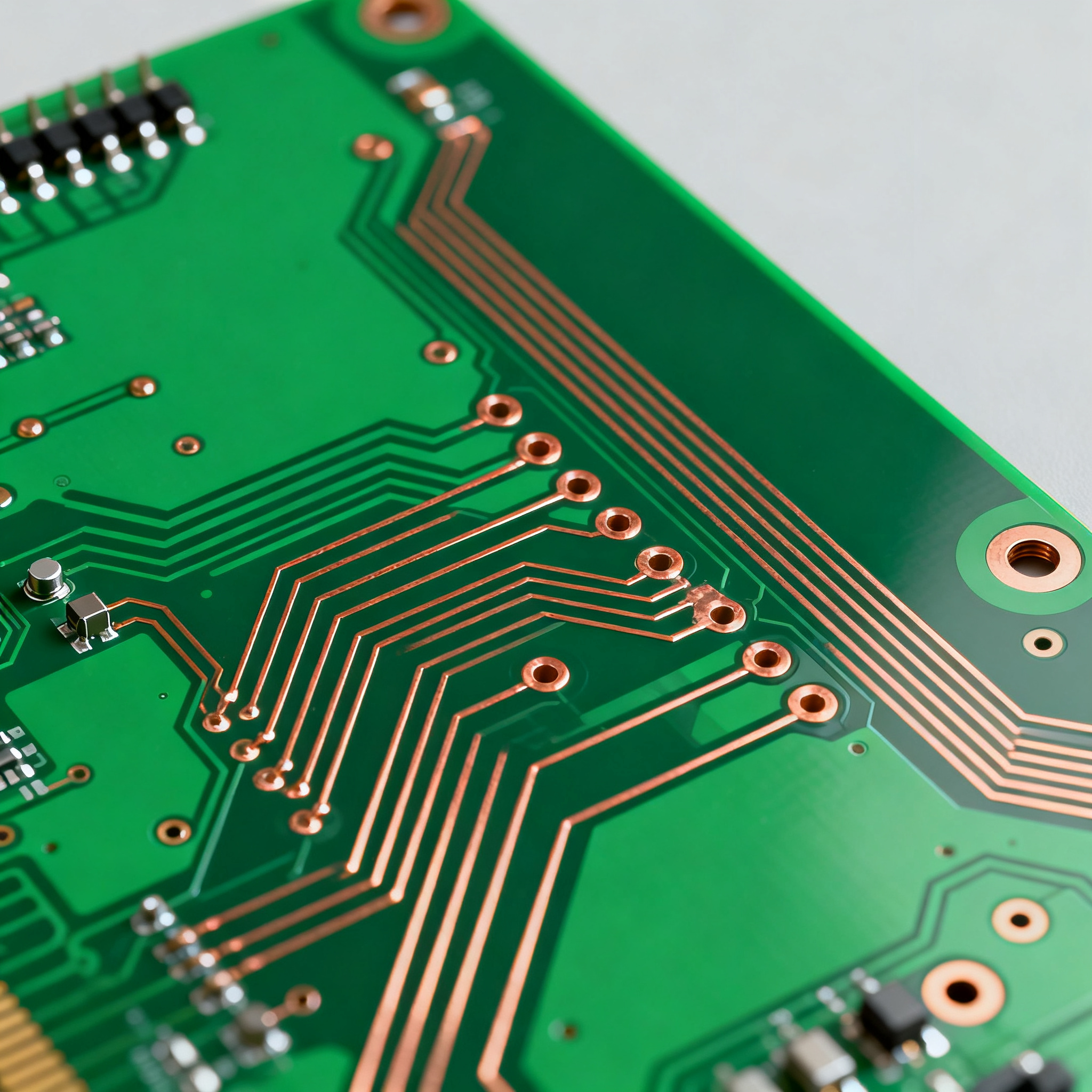
The architecture of a PCB is a complex interconnection of components, traces, and layers designed to support electronic circuits. Core concepts include the layout design, which involves the strategic placement of components to optimize performance and minimize interference. The principles of signal integrity, thermal management, and power distribution play vital roles in the effectiveness of the PCB. Moreover, adherence to IPC standards ensures quality and reliability in both design and manufacturing. Understanding these principles is crucial for selecting the right components, like IC chips, and ensuring they meet the required specifications for your application.
Detailed Specifications
When designing a PCB, understanding component specifications is crucial. These specifications include parameters like CPU speed, memory, and power requirements, which directly influence the performance and compatibility of the IC chips. Datasheets provide detailed insights into these specifications, helping engineers make informed decisions during the selection process. Below is a table illustrating core specifications of a typical IC chip used in PCB designs.
| Specification | Description | Value |
|---|---|---|
| CPU Speed | Maximum operating frequency | 1.2 GHz |
| Memory | Integrated RAM | 256 KB |
| Flash | Non-volatile storage | 2 MB |
| Peripherals | Available interfaces | UART, SPI, I2C |
| Power Supply | Operating voltage range | 3.3V |
| Package Type | Physical chip package | LQFP-48 |
| Operating Temperature | Temperature range for operation | -40°C to 85°C |
| Dimensions | Physical size of the chip | 7x7 mm |
| ADC Channels | Number of ADC inputs | 16 |
| DAC Channels | Number of DAC outputs | 2 |
| Connectivity | Wireless communication options | WiFi, Bluetooth |
| Cost | Approximate unit price | $5.00 |
Key Takeaways from the Specifications
The core specifications listed above highlight the capabilities and limitations of the IC chip. The CPU speed and memory are critical for processing power and data handling, impacting the overall performance of the PCB. Peripherals such as UART, SPI, and I2C provide essential communication interfaces, enabling integration with other components. The power supply requirements and operating temperature range are crucial for ensuring compatibility with the PCB's power management system. Understanding these specifications allows engineers to select the right IC chip for their application, balancing performance, cost, and power efficiency.
| Parameter | Condition | Value |
|---|---|---|
| Supply Voltage | Typical operation | 3.3V |
| Input Voltage Range | All I/O pins | 0V to 3.6V |
| Output High Voltage | IOH = -4 mA | 2.9V |
| Output Low Voltage | IOL = 4 mA | 0.4V |
| Input Leakage Current | VIN = 0V to 3.6V | ±1 µA |
| Operating Current | Active mode | 30 mA |
| Standby Current | Low-power mode | 5 µA |
| Propagation Delay | Maximum load | 5 ns |
| Rise Time | Standard load | 2 ns |
| Fall Time | Standard load | 2 ns |
| ESD Protection | All pins | ±2000 V |
| Thermal Resistance | Junction to ambient | 40°C/W |
Practical Implications
The electrical characteristics table provides insights into the operational parameters of the IC chip. The supply voltage and input voltage range are fundamental for ensuring proper power management. Output voltage levels indicate the logic thresholds for high and low states, essential for signal integrity. The operating current and standby current highlight the chip's power consumption, which is critical for battery-powered applications. Propagation delay, rise time, and fall time affect the timing performance of the chip, influencing the speed of data processing. Understanding these parameters helps engineers optimize their PCB designs for efficiency and reliability.
| Application | Configuration | Benefits |
|---|---|---|
| Embedded Systems | Standalone MCU | Low power, high integration |
| IoT Devices | Wireless connectivity | Remote control, monitoring |
| Consumer Electronics | Multimedia processing | High performance, cost-effective |
| Industrial Automation | Robust design | Reliable, extended temperature range |
| Automotive | Real-time processing | Safety, efficiency |
| Medical Devices | Precision measurement | Accurate, safe |
| Wearables | Compact form factor | Lightweight, portable |
| Smart Home | Integrated sensors | Convenience, energy-saving |
Application Guidelines
The application comparison table illustrates the versatility of the IC chip across various domains. In embedded systems, the chip's low power and high integration make it ideal for compact designs. IoT devices benefit from its wireless connectivity, enabling remote control and monitoring. Consumer electronics leverage its multimedia processing capabilities for enhanced performance. The chip's robust design suits industrial automation applications, where reliability is paramount. In automotive and medical applications, real-time processing and precision measurement are critical, ensuring safety and accuracy. Selecting the right configuration based on application requirements ensures optimal performance.
Design Considerations
Designing a custom PCB involves several critical considerations. First, component placement must ensure minimal signal interference and effective heat dissipation. Traces should be routed to maintain signal integrity, avoiding sharp angles and ensuring sufficient spacing. Power distribution networks must be carefully designed to prevent voltage drops and ensure stable operation. Thermal management is crucial, especially for high-performance IC chips, requiring the use of heat sinks or thermal vias. Compliance with IPC standards ensures quality and reliability, guiding the design process from schematic capture to layout. By considering these factors, engineers can create PCBs that meet performance, cost, and reliability goals.
Step-by-Step Implementation
- Conceptualization: Define the objectives and requirements of your PCB design, including the selection of IC chips and other components.
- Schematic Design: Create a schematic diagram that represents the electrical connections between components, ensuring proper functionality.
- Component Selection: Choose components based on specifications and datasheets, ensuring compatibility with the PCB's requirements.
- PCB Layout: Design the physical layout of the PCB, placing components strategically to optimize performance and minimize interference.
- Design Rule Check (DRC): Perform a DRC to ensure the layout adheres to industry standards and design guidelines.
- Prototype Fabrication: Send the design files to a PCB manufacturer to create a prototype for testing and validation.
- Testing and Validation: Test the prototype to ensure it meets performance specifications and make necessary adjustments.
- Production: Once validated, proceed to full-scale production, ensuring quality control at every stage.
Common Issues & Solutions
- Signal Integrity Problems: Use differential signaling and proper trace routing to minimize crosstalk and EMI.
- Thermal Management: Implement heat sinks, thermal vias, and proper airflow to dissipate heat effectively.
- Power Distribution: Design robust power planes to prevent voltage drops and ensure stable power supply.
- Component Placement Errors: Utilize automated placement tools to optimize component layout and reduce manual errors.
- Manufacturing Defects: Conduct thorough inspections and testing to identify and rectify defects early in the process.
- Compliance Issues: Adhere to IPC standards and regulations to ensure compliance and avoid redesigns.
Applications & Use Cases
PCBs are integral to various applications, from consumer electronics to industrial systems. In consumer electronics, they enable compact, high-performance devices like smartphones and tablets. In industrial automation, PCBs are used in control systems for machinery and robotics, ensuring reliability and efficiency. Automotive applications rely on PCBs for engine control units and infotainment systems, enhancing safety and user experience. Medical devices use PCBs for precise monitoring and diagnostics, ensuring accuracy and reliability. The versatility of PCBs makes them indispensable in modern technology.
Selection & Sourcing Guide
When selecting IC chips and other components for your PCB design, consider factors such as performance, cost, and compatibility. Utilize resources like IC Online to compare specifications and prices from various manufacturers. Ensure that components meet industry standards and are available in the required quantities for your production needs. Collaborate with suppliers to ensure timely delivery and support during the design and manufacturing process.
FAQ
- What are the key factors to consider when selecting an IC chip for a PCB? Consider performance specifications, power requirements, compatibility, and cost.
- How do I ensure signal integrity in my PCB design? Use proper trace routing, differential signaling, and impedance matching techniques.
- What is the importance of thermal management in PCB design? Effective thermal management prevents overheating, ensuring reliable operation and longevity.
- How can I reduce manufacturing defects in my PCB? Conduct thorough design rule checks and use automated inspection tools.
- What role do IPC standards play in PCB design? IPC standards ensure quality, reliability, and compliance with industry regulations.
- How do I select the right components for my PCB design? Use datasheets and specifications to ensure compatibility and performance.
- What are the benefits of prototyping a PCB design? Prototyping allows for testing and validation, identifying issues before full-scale production.
- How can I optimize power distribution in my PCB design? Design robust power planes and use decoupling capacitors to maintain stable power supply.
- What are the common challenges in PCB fabrication? Challenges include signal integrity, thermal management, and compliance with standards.
- How do I ensure my PCB design meets industry standards? Follow IPC guidelines and conduct regular audits to ensure compliance.
Conclusion
Designing and fabricating a custom PCB is a complex process that requires careful planning and execution. By understanding component specifications, adhering to industry standards, and following best practices, you can create reliable and efficient PCBs for various applications. This guide provides the essential knowledge and tools needed to navigate the PCB fabrication process from concept to production, ensuring success in your electronic design projects.