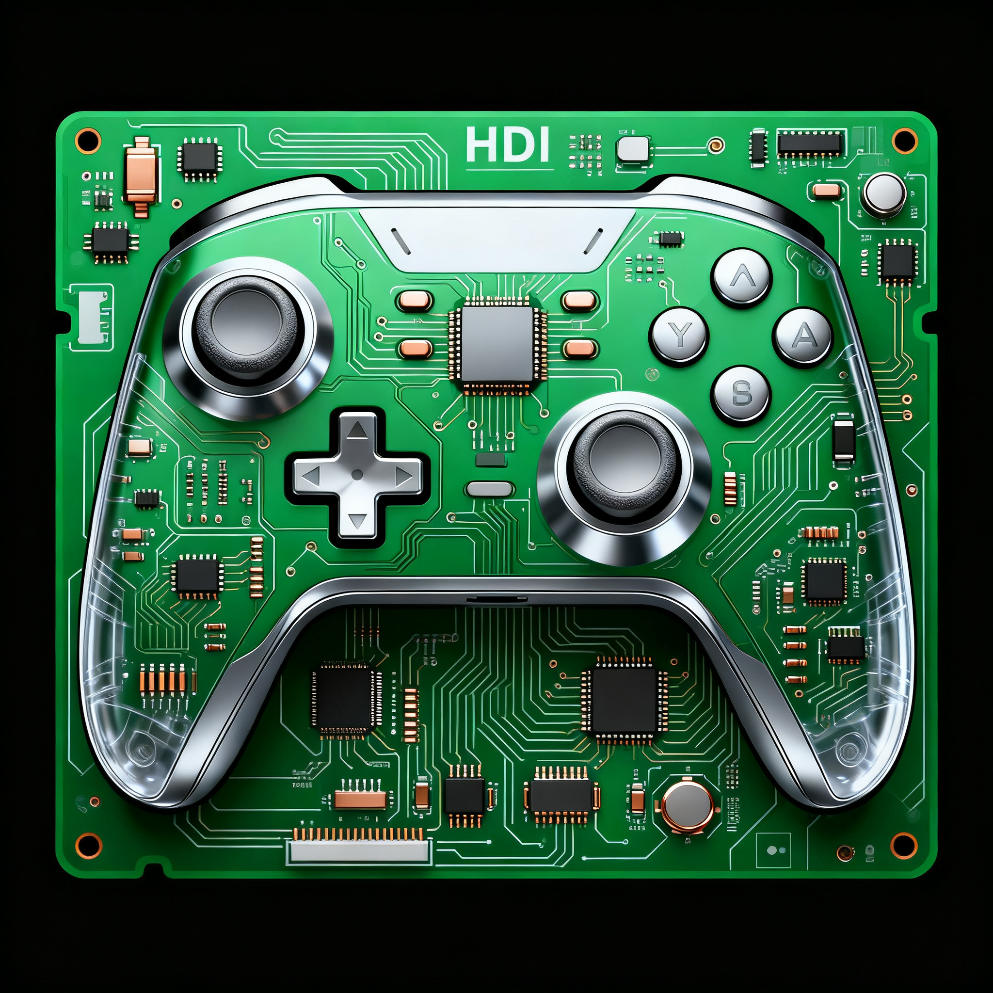
Step-by-Step Design Tutorial: HDI PCB Layout for Next-Gen Gaming Console Controllers
Why Next-Gen Game Controllers Demand HDI: Size, Speed, and Wireless Constraints Modern gaming controllers have evolved far beyond simple button-and-joystick peripherals. The latest flagship devices—th...
Why Next-Gen Game Controllers Demand HDI: Size, Speed, and Wireless Constraints
Modern gaming controllers have evolved far beyond simple button-and-joystick peripherals. The latest flagship devices—think Sony DualSense, Xbox Elite Wireless, and premium third-party pads—pack haptic voice-coil actuators, adaptive triggers with precision force feedback, multi-channel Bluetooth/2.4 GHz radios, high-resolution touchpads, and 32-bit ARM MCUs with 200+ pins into enclosures barely 15 mm thick. This integration density, combined with aggressive industrial design that leaves no room for bulky connectors or large keep-out zones, forces a fundamental shift from conventional through-hole or standard multilayer PCBs to High-Density Interconnect (HDI) technology.
The pain points are immediate. A typical next-gen controller mainboard must route DDR memory interfaces to a BGA processor, manage sensitive RF feedlines for Bluetooth and proprietary low-latency wireless, and distribute power to multiple haptic drivers—all on a board that often measures less than 60 × 40 mm. Traditional 4-layer boards with mechanical drilled vias simply cannot fan out a 0.4 mm-pitch BGA without consuming excessive layers or violating impedance control. As Altium’s HDI design basics emphasize, routing efficiencies for HDI depend critically on stackup, via architecture, and BGA fanout strategy. Without microvias and buried structures, you’ll either sacrifice signal integrity or inflate the board outline beyond the controller’s ergonomic envelope.
Wireless coexistence adds another layer of complexity. A controller must maintain a robust Bluetooth link while operating in the crowded 2.4 GHz ISM band, often alongside Wi-Fi and other peripherals. Any impedance discontinuity on the antenna feedline, excessive crosstalk from digital traces, or poorly stitched return paths can degrade sensitivity and range. HDI’s ability to place ground-reference planes immediately adjacent to signal layers and to stitch them with laser-drilled microvias every few millimeters is no longer a luxury—it’s a requirement for meeting the 50 Ω ±10% target across the antenna path. PCBSync’s comprehensive HDI guide notes that proper stackup design can reduce board size by up to 60% while improving signal integrity, a combination that aligns perfectly with the controller’s dual mandate of compactness and wireless performance.
Thermal management, though often overlooked in battery-powered devices, also benefits from HDI. Haptic drivers can draw several amps during intense feedback events, and the MCU’s core voltage regulator generates localized heat. HDI’s thin dielectrics and copper-filled microvias provide lower thermal resistance paths to internal ground planes, helping to spread heat without dedicated heatsinks. For the design team, the message is clear: if you’re developing a controller that must feel responsive, connect reliably, and fit in a palm-sized shell, HDI isn’t optional—it’s the baseline.
HDI Stackup Essentials: Microvias, Buried Vias, and Layer Pairing for Controller PCBs
At the heart of any HDI design lies the microvia. Unlike traditional mechanically drilled vias with diameters of 0.2 mm or larger, laser-drilled microvias typically range from 0.1 mm to 0.15 mm and span only one dielectric layer. This small footprint enables via-in-pad placement directly under BGA balls, eliminating the dog-bone fanout that wastes routing space. In a controller board, where the main processor often uses a 0.4 mm-pitch BGA, via-in-pad with stacked microvias is the most efficient way to escape signals to inner layers.
Buried vias, formed by mechanically drilling and plating core layers before lamination, connect two or more internal layers without penetrating the outer surfaces. They are essential for building complex layer-to-layer interconnects in 6- to 10-layer stackups without consuming real estate on the top and bottom. Staggered microvias offset each layer’s via pad slightly to avoid alignment issues, while stacked microvias align precisely on top of each other, offering the highest density but demanding tighter registration control from the fabricator. The choice between staggered and stacked structures directly impacts yield and cost.
Dielectric material selection is governed by IPC/JPCA-4104, which specifies qualification and performance requirements for HDI substrates. For controller applications, low-loss materials like Isola FR408HR or Panasonic Megtron 6 are often chosen for RF layers, while standard FR-4.1 may suffice for digital-only cores. The table below summarizes the via types and typical layer pairing strategies you’ll encounter when designing a 6–10 layer controller board, drawing on practical guidelines from HDI PCB layout references.
| Via Type | Structure | Typical Aspect Ratio | Recommended Layer Pairing | Notes for Controller PCBs |
|---|---|---|---|---|
| Through-hole (mechanical) | Drilled through entire board | 10:1 max | All layers | Use only for connectors and test points; avoid under BGAs. |
| Blind microvia (laser) | Outer layer to adjacent inner layer | 1:1 (depth ≤ 0.1 mm) | L1–L2, L8–L7 (example) | Ideal for BGA fanout; via-in-pad capable. |
| Buried via (mechanical) | Internal layer to internal layer | 8:1 typical | L2–L7, L3–L6 | Connects power/ground planes; keep diameter ≥ 0.2 mm. |
| Stacked microvia (1-N-1) | L1–L2 microvia stacked on L2–L3 buried via | 1:1 per segment | L1–L2–L3 | Highest density for 0.4 mm-pitch BGAs; requires precise registration. |
| Staggered microvia | L1–L2 microvia offset from L2–L3 buried via | 1:1 per segment | L1–L2, then L2–L3 with offset | More forgiving in fabrication; slightly larger area. |
| Skip via (laser) | Outer layer to layer N+2 (skipping one layer) | 1:1.5 | L1–L3 | Rare in controllers; used for thick dielectrics. |
When pairing layers, a common 8-layer controller stackup might look like: L1 (top signal, RF), L2 (GND), L3 (signal), L4 (power), L5 (GND), L6 (signal), L7 (GND), L8 (bottom signal). Laser microvias connect L1–L2 and L7–L8, while buried vias link L2–L7 for power distribution. This arrangement keeps RF return paths tight and isolates sensitive analog signals. Always verify with your fabricator that the chosen dielectric thicknesses support the required 50 Ω and 90 Ω differential impedances on outer and inner layers.
Stackup Showdown: 1-N-1 vs. 2-N-2 vs. 3-N-3 for Controller Density and Cost
Not every controller needs the most aggressive HDI architecture. The decision between 1-N-1, 2-N-2, and 3-N-3 stackups hinges on BGA pitch, routing channel requirements, and budget. A 1-N-1 build uses a single microvia layer on each side of a conventional multilayer core, while 2-N-2 adds a second microvia layer, enabling stacked or staggered structures that reach deeper into the board. 3-N-3 extends this further but is rarely justified in a handheld controller unless you’re integrating a complex FPGA or massive memory bus. The table below compares these architectures using cost-optimization insights from AllPCB’s HDI price calculator and manufacturability advice from Matric’s six key design guidelines.
| Comparison Metric | 1-N-1 | 2-N-2 | 3-N-3 | Selection Criteria & Failure Boundary |
|---|---|---|---|---|
| Microvia layers per side | 1 | 2 | 3 | Match to BGA depth; 1-N-1 handles 0.8 mm pitch easily. |
| Via-in-pad capability | Yes (single-level) | Yes (stacked or staggered) | Yes (complex stacked) | 2-N-2 needed for 0.4 mm-pitch BGAs with full via-in-pad. |
| Typical total layer count | 4–6 | 6–8 | 8–12 | Choose 2-N-2 for 8-layer controller with dense RF and digital. |
| Routing channel availability | Moderate; dog-bone may be required | High; full matrix breakout possible | Very high; overkill for controllers | 2-N-2 allows 2–3 traces between 0.4 mm BGA pads. |
| Fabrication cost multiplier | 1.2–1.5× over standard | 1.8–2.5× | 3×+ | For volumes >50k, 2-N-2 premium narrows; NRE dominates. |
| Typical NRE (prototype) | $800–$1,500 | $1,500–$3,000 | $3,000–$6,000 | 2-N-2 NRE includes two lamination cycles and laser drilling. |
| Signal integrity (RF) | Good with careful stackup | Excellent; reference plane adjacency | Over-designed | 2-N-2 provides solid ground stitching for 2.4 GHz. |
| Assembly yield risk | Low | Moderate; voiding in stacked vias | Higher; delamination risk | Use qualified fabricator with plasma desmear for 2-N-2. |
For the vast majority of next-gen controller designs, a 2-N-2 stackup on an 8-layer board hits the sweet spot. It provides enough routing channels to fan out a 0.4 mm-pitch BGA without resorting to extra layers, supports via-in-pad for all critical signals, and keeps the RF feedline well-shielded. 1-N-1 may suffice for simpler controllers with 0.8 mm-pitch MCUs and fewer haptic channels, but you’ll likely need dog-bone fanout that consumes board area. 3-N-3, while technically impressive, introduces additional lamination cycles that raise cost and yield risk without tangible benefit for a battery-powered handheld device. Always run a cost-benefit analysis with your CM early in the design phase; the per-unit cost difference between 2-N-2 and 1-N-1 can drop below 20% at production volumes above 100k units.
A Step-by-Step Layout Walkthrough: From Schematic to Gerber for an HDI Controller Board
Let’s walk through a practical HDI layout flow for a hypothetical next-gen controller mainboard featuring a 0.4 mm-pitch BGA MCU, a Bluetooth/2.4 GHz radio, USB 2.0 interface, and multiple haptic driver ICs. The target stackup is an 8-layer 2-N-2 with ENIG finish. We’ll use Altium Designer, but the principles apply to any advanced PCB tool. This sequence draws on JHYPCB’s HDI layout guide and Aivon’s beginner-focused design walkthrough.
1. Stackup Definition and Material Selection
Open the Layer Stack Manager and define an 8-layer stackup: Top (signal), GND1, Signal2, Power3, GND4, Signal5, GND6, Bottom (signal). Assign 0.1 mm (4 mil) prepreg between L1–L2 and L7–L8 for laser microvias. Core thicknesses should yield 50 Ω single-ended and 90 Ω differential impedances after consulting your fabricator’s impedance calculator. Select low-loss prepreg (e.g., Isola 370HR) for the RF layers. Save this stackup as a template for reuse.
2. BGA Fanout and Via Planning
Place the MCU BGA and set the grid to 0.1 mm. For a 0.4 mm-pitch device, you’ll need via-in-pad on the outer rows and possibly the inner rows if the pin count exceeds what dog-bone can handle. Use stacked microvias (L1–L2–L3) for power and ground balls to reach the internal planes quickly. For signal balls, a staggered approach (L1–L2 microvia, then a short trace to an L2–L3 buried via) can save cost if your fabricator’s registration capability is tight. Define via types in the design rules: laser via pad size 0.25 mm, hole 0.1 mm; buried via pad 0.45 mm, hole 0.2 mm. Run the fanout autorouter as a starting point, then manually optimize to avoid via stubs on high-speed lines.
3. Differential Pair Routing for USB and Antenna
USB 2.0 requires a 90 Ω differential pair. Route the D+/D- traces on L1 with a solid GND reference on L2, keeping the pair length matched within 0.5 mm. For the Bluetooth antenna feedline, implement a coplanar waveguide (CPW) structure on the top layer: a 50 Ω trace with ground pour on either side, stitched to L2 GND with microvias every 2 mm. Use Altium’s impedance profile to calculate trace width and spacing based on your stackup. Avoid routing digital traces parallel to the antenna feedline; maintain at least 3× the trace-to-copper clearance. Simulate the feedline with a 2.5D solver if possible.
4. Power Distribution and Haptic Routing
Haptic drivers can draw 2–3 A peaks. Use wide polygons on L4 (power) and stitch to L2/L6 GND with multiple buried vias. Place decoupling capacitors directly under the BGA on the bottom layer, connecting through microvias to minimize loop inductance. For adaptive trigger motors, route differential pairs with 100 Ω impedance if using PWM control.
5. Design Rule Setup and DFM Verification
Define clearances and widths according to IPC-6016 Class 2 for HDI. The table below summarizes a typical rule set for a 2-N-2 controller board. Run a full DRC, paying special attention to microvia annular ring requirements (minimum 0.075 mm) and copper-to-edge distances. Generate Gerbers with separate files for each laser drill layer and mechanical drill layer. Include a detailed fabrication drawing specifying stackup, impedance requirements, and via types.
| Parameter | Recommended Value | Unit | Notes |
|---|---|---|---|
| Minimum trace/space (outer) | 3/3 (75/75) | mil (µm) | For Class 2; 2.5/2.5 possible with tight process control |
| Minimum trace/space (inner) | 3.5/3.5 | mil | Relax slightly for buried layers |
| Laser via pad size | 0.25 (0.1 hole) | mm | Via-in-pad on 0.4 mm BGA |
| Buried via pad size | 0.45 (0.2 hole) | mm | Mechanical drill |
| Microvia annular ring | ≥ 0.075 | mm | Per IPC-6016 Class 2 |
| Impedance tolerance | ±10% | Ω | 50 Ω single-ended, 90 Ω USB, 100 Ω diff |
| Copper-to-board edge | 0.4 | mm | For router tolerance |
| Solder mask dam width | 0.1 | mm | Between via-in-pad and adjacent pads |
Before releasing to fabrication, perform a final checklist: all BGA pins escaped, no floating planes, antenna keep-out zone respected, and all differential pairs length-tuned. Engage your assembly partner early—NovaPCBA, for instance, offers HDI-specific assembly services including X-ray inspection for stacked microvias and ENIG/ENEPIG surface finishes that ensure reliable soldering of fine-pitch BGAs. Their quick-turn prototyping can validate your 2-N-2 design in as little as 10 days.
Controller HDI Design FAQs: Signal Integrity, Assembly Yield, and Cost Tradeoffs
Q: What minimum trace/space can I reliably use on a 2-N-2 HDI controller board?
A: For IPC-6016 Class 2, 3/3 mil (75/75 µm) is widely achievable with modern laser direct imaging and etching. If your design includes a 0.4 mm-pitch BGA, you may need 2.5/2.5 mil traces to escape inner rows. Confirm with your fabricator’s capabilities—registration accuracy of the laser drill and copper plating uniformity directly affect yield at these dimensions. Always specify the performance class on the fabrication drawing.
Q: How do I prevent signal integrity issues on the Bluetooth antenna feedline in a mixed-signal HDI stackup?
A: Use a coplanar waveguide with ground stitching vias on either side of the trace, spaced no more than λ/10 at 2.4 GHz (about 2.5 mm). Maintain a solid, unbroken reference plane directly beneath the feedline on L2. Keep all digital traces and power shapes out of the antenna keep-out area. Simulate the structure with a 2.5D field solver to hit 50 Ω ±10%. Avoid via stubs by routing the feedline entirely on the top layer; if a layer transition is unavoidable, use a back-drilled via or a microvia to eliminate the stub.
Q: What via structure works best for a 0.4 mm-pitch BGA in a game controller?
A: Via-in-pad with stacked microvias (1-N-1 or 2-N-2) is the most compact solution. For a 2-N-2 stackup, you can place a laser via directly on the BGA pad, drop to L2, and then either stack a second microvia to L3 or route a short trace to a buried via. If cost is a primary concern, staggered microvias with dog-bone routing on outer layers can work but may force an increase in layer count or board size. Most controller designs benefit from the density of stacked vias.
Q: How does HDI layer count impact assembly yield and rework?
A: Higher layer counts and stacked microvias increase the risk of voiding, delamination, and thermal stress during reflow. The additional lamination cycles in 2-N-2 and 3-N-3 builds can trap moisture or contaminants if not properly handled. Mitigate these risks by selecting a fabricator with controlled laser drilling and plasma desmear processes. For assembly, specify ENIG or ENEPIG surface finish to ensure flat pads for fine-pitch BGAs, and use X-ray inspection to verify via-in-pad solder joint integrity. Rework of a failed BGA on an HDI board is extremely difficult; design for testability and consider edge-bonding for mechanical robustness.
Q: What are typical NRE and per-unit cost differences between a standard 4-layer and a 6-layer 2-N-2 HDI board for a controller?
A: NRE for a 2-N-2 prototype run typically falls between $1,500 and $3,000, covering tooling, laser drilling, and two lamination cycles. Per-unit costs at low volumes (100–500 pieces) can be 30–50% higher than a standard 4-layer board of similar size. At production quantities above 50,000 units, the premium narrows to 15–25% as material and process efficiencies scale. The exact numbers depend on board dimensions, material selection, and surface finish; always request a quote from your CM early in the design cycle.
Q: Can I use HDI for a controller with flex-rigid sections?
A: Yes, but it demands careful stackup symmetry and material compatibility. The rigid section can employ a 2-N-2 HDI stackup, while the flex layer typically uses adhesive-less polyimide with a simpler via structure. You’ll need to coordinate with the fabricator to match the flex-layer via pad sizes with the rigid microvia pads and to manage the transition zone where rigid and flex meet. Plan for a symmetrical build to prevent warpage during reflow, and use strain relief at the rigid-flex interface to avoid trace cracking under mechanical stress.
Designing an HDI controller board is a multidisciplinary challenge that rewards early collaboration with your fabrication and assembly partners. By selecting the right stackup, rigorously managing impedance, and adhering to proven DFM rules, you can deliver a controller that feels responsive, connects seamlessly, and survives the rigors of daily gaming. For teams looking to accelerate their HDI development cycle, NovaPCBA offers integrated PCB fabrication and assembly services with expertise in 2-N-2 and flex-rigid HDI builds, helping you move from concept to volume production with confidence.
References & Further Reading
- Altium – What's HDI? Design Basics and the HDI PCB Manufacturing Process
- PCBSync – HDI PCB Design and Manufacturing: From Basics to Advanced Techniques
- Matric – HDI PCB Design Guidelines for Layout & Manufacturability
- AllPCB – HDI PCBs: Benefits, Design Tips, and Manufacturing Techniques
- Sierra Circuits – Design for HDI (IPC/JPCA-4104)
- HDI PCB – HDI PCB Layout and Basic HDI Design Guidelines
- JHYPCB – HDI PCB Layout and Basic HDI Design Guidelines
- Aivon – HDI PCB Design Guide for Beginners
- NovaPCBA – HDI PCB Fabrication and Assembly Services
- IPC-6016 – Qualification and Performance Specification for High Density Interconnect (HDI) Structures