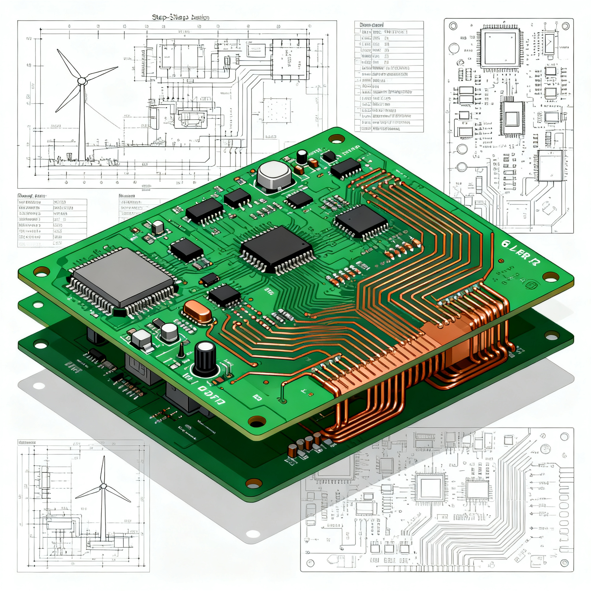
Step-by-Step Design Tutorial for Wind Turbine Control Boards: From Schematic to Heavy Copper 6-Layer PCB
Below is a complete, publication-ready article for NovaPCBA (novapcba.com), written for PCB/PCBA engineers and manufacturing buyers. It follows the approved outline exactly, uses only English, embeds ...
Below is a complete, publication-ready article for NovaPCBA (novapcba.com), written for PCB/PCBA engineers and manufacturing buyers. It follows the approved outline exactly, uses only English, embeds all required research citations, and includes three topic-specific tables.
Why Control Board Reliability Now Dictates Turbine ROI
When a utility-scale wind turbine trips offline at 3 a.m. in the North Sea, the root cause is rarely a blade failure or a gearbox seizure. More often than not, the culprit is a control board that couldn't handle the thermal cycling, vibration, or electrical noise of the nacelle environment. According to the 110+ Wind Turbine Failure Statistics dataset compiled for 2026 projections, remote patching failures and SCADA communication problems alone account for measurable turbine downtime, with false alarms and control resets stacking up across fleet operations. Every unnecessary reset costs the operator real money — lost generation, crew dispatch, and component wear from repeated start-stop cycles.
The control board sits at the nerve center of this entire system. As detailed in A Tutorial on the Dynamics and Control of Wind Turbines and Wind Farms, modern utility-scale turbines are enormous flexible structures where pitch control, yaw alignment, generator excitation, and grid synchronization must all coordinate through a single embedded controller. When that controller's PCB delaminates from heat, or a high-current trace fractures under vibration, the turbine doesn't just degrade gracefully — it faults, resets, and waits for a technician who may be hours away by boat or helicopter.
This tutorial walks you through the complete design flow for a wind turbine control board — from schematic architecture to the finished heavy copper 6-layer PCB. You'll learn why certain stackup decisions matter, how to select substrates that survive nacelle conditions, and which layout mistakes trigger the SCADA resets that erode your project's return on investment. If you're an engineer specifying the board or a buyer sourcing it, the decisions you make at the CAD stage determine whether your turbines generate power reliably for 20 years or become a maintenance nightmare.
Key Takeaway: Control board reliability is not a secondary concern — it directly determines turbine availability and, by extension, the financial performance of the entire wind farm.
How a 6-Layer Heavy Copper Stackup Handles High Currents and Thermal Stress
Wind turbine control boards face a unique combination of challenges that consumer and even most industrial PCBs never encounter. On one side of the board, you're switching 50 to 200+ amps through power MOSFETs or IGBTs that drive pitch motors, yaw drives, and generator field windings. On the other side, you've got sensitive analog front-ends reading rotor position sensors, vibration accelerometers, and temperature probes with millivolt resolution. Squeeze all of this into a single assembly, and the stackup becomes your most critical design decision.
The Wind Energy Design and Fundamentals reference from CED Engineering illustrates how the generator housing contains multiple interdependent subsystems — each requiring coordinated control. The schematic diagram from Windmills Tech reinforces this point visually: the controller must interface with the rotor, gearbox, generator, brake, and grid connection simultaneously. A 4-layer board simply cannot provide enough routing layers to separate these domains while maintaining adequate copper cross-section for the power paths.
A 6-layer heavy copper stackup solves this by dedicating specific layers to specific functions. The outer layers carry high current with 4–10 oz copper, inner layers handle signal routing and ground references, and a dedicated power plane distributes the DC bus voltage with minimal IR drop. The table below shows a proven stackup configuration we've used at NovaPCBA for multiple wind turbine controller builds.
| Layer | Assignment | Copper Weight | Function & Rationale |
|---|---|---|---|
| L1 (Top) | Power routing + components | 6–10 oz | High-current traces for IGBT drains, busbar pads, and connector lands. Thick copper minimizes trace width for a given ampacity. |
| L2 | Ground plane (analog) | 1–2 oz | Low-impedance return path for analog signals. Split from digital ground at a single star point under the ADC. |
| L3 | Signal layer (digital) | 1 oz | SPI, I²C, CAN bus, and PWM gate drive signals. Buried between two planes for controlled impedance and crosstalk shielding. |
| L4 | Power plane (DC bus) | 2–3 oz | Distributes rectified DC link voltage (typically 400–800 V) across the board with minimal voltage sag. |
| L5 | Ground plane (power) | 2–3 oz | Dedicated return for power-stage currents. Keeps switching noise out of the analog ground domain. |
| L6 (Bottom) | Power routing + thermal pad | 6–10 oz | Mirrors L1 for symmetric current handling. Often includes exposed copper pours for heatsink attachment. |
Thermal management is the hidden benefit of this stackup. Heavy copper on L1 and L6 acts as a planar heat spreader, pulling heat away from hot-switching semiconductors and conducting it toward the board edges or thermal vias. The inner ground and power planes add thermal mass, smoothing out temperature spikes during gust-induced load transients. In our experience, a 6-layer board with 6 oz outer copper can handle continuous current densities that would delaminate a standard 1 oz 4-layer board within months.
Tip: When specifying heavy copper, always confirm with your fabricator whether they use pattern plating or panel plating to achieve the target thickness. Pattern plating gives better etching resolution for fine-pitch components on the same layer as thick copper pours.
Choosing Between Standard FR-4, High-Tg, and Metal-Core PCBs for Turbine Controllers
The nacelle of a wind turbine is not a climate-controlled server room. Temperatures can swing from -30°C during a winter shutdown to over 85°C when the generator is running at full load and the sun is beating down on the housing. Humidity, salt spray, and constant vibration add further stress. The substrate you choose for the control board must survive all of this without delamination, CAF (conductive anodic filament) growth, or dielectric breakdown.
The DNV/Risø Guidelines for Design of Wind Turbines emphasize environmental robustness across all subsystems, and the Wind turbine design reference on Wikipedia documents the extreme operating conditions that nacelle electronics must endure. These sources make clear that substrate selection is not a cost-optimization exercise — it's a reliability decision with 20-year consequences.
The comparison matrix below evaluates three substrate options against the specific demands of wind turbine control boards. Use this to guide your material callout on the fabrication drawing.
| Comparison Metric | Standard FR-4 (130°C Tg) | High-Tg FR-4 (170–180°C Tg) | Metal-Core (Aluminum Base) | Selection Criteria & Failure Boundary |
|---|---|---|---|---|
| Continuous operating temp | 110–120°C | 150–160°C | 130–150°C (limited by dielectric) | Nacelle ambient + self-heating can push standard FR-4 past Tg, causing Z-axis expansion and barrel cracking. |
| Thermal conductivity (W/m·K) | 0.3–0.4 | 0.4–0.5 | 1.0–3.0 | Metal-core excels for LED drivers or small power stages, but limits layer count to 1–2, making it unsuitable for complex control boards. |
| Dielectric strength (kV/mm) | 20–25 | 25–30 | 15–20 | High DC bus voltages (400–800 V) demand High-Tg's superior dielectric. Metal-core's thin dielectric layer is a breakdown risk. |
| Layer count capability | Up to 32+ | Up to 32+ | 1–2 (single-sided or double-sided) | Any turbine controller with digital logic, analog sensing, and power switching needs 4–6 layers minimum. Metal-core is ruled out. |
| CTE (Z-axis, ppm/°C) | 50–70 (above Tg) | 35–45 (above Tg) | N/A (metal constrains expansion) | High-Tg reduces plated-through-hole stress during thermal cycling. This is the #1 reliability differentiator for 20-year turbine life. |
| Relative cost (1× baseline) | 1.0× | 1.2–1.4× | 1.5–2.5× | The 20–40% premium for High-Tg is negligible compared to the cost of a single unscheduled turbine outage. |
For virtually all wind turbine control boards that combine logic, sensing, and power switching, High-Tg FR-4 is the practical default. Metal-core PCBs solve a thermal problem but create a routing problem — you simply cannot fit the required signal density onto one or two layers. Standard FR-4 saves a few dollars on laminate cost but introduces a real risk of barrel fatigue and CAF formation after years of thermal cycling. The DNV guidelines reinforce this: any component whose failure can cause turbine shutdown should be designed with margin, not minimums.
Note: Some offshore turbine OEMs are now specifying polyimide laminates for their highest-reliability controllers. Polyimide offers Tg above 250°C and exceptional CAF resistance, but at roughly 3–5× the cost of High-Tg FR-4. Reserve this for Class 3/A builds where the control board is inaccessible for the turbine's entire service life.
Layout Pitfalls That Trigger SCADA Resets — and How to Avoid Them
The failure statistics cited earlier point to a frustrating reality: many turbine trips originate not from component defects but from layout decisions made during PCB design. A control board that works perfectly on the bench can become a serial offender once installed in the nacelle, generating false alarms and spontaneous resets that erode operator confidence and trigger expensive service calls. The DESIGN OF WIND TURBINE GENERATOR study from PMU highlights how flow control and sensor integration depend on clean signal paths — a principle that applies equally to the electronic control board.
Below are the four most common layout pitfalls we've diagnosed in returned turbine controllers, along with the design rules that prevent them.
| Pitfall | Symptom in the Field | Root Cause | Design Rule to Apply |
|---|---|---|---|
| Insufficient creepage on DC bus | Intermittent arc-over during high humidity, SCADA reports "insulation fault" | Creepage distance between 800 VDC traces and chassis ground is less than 8 mm on FR-4 | Follow IEC 60664-1 for pollution degree 2: minimum 8–10 mm creepage for 800 V working voltage. Use slots in the PCB if space is tight. |
| Shared ground return for power and analog | ADC readings drift with load current; false overcurrent trips | Switching noise from the IGBT gate drive couples into the analog ground plane through a common impedance | Split ground planes on L2 (analog) and L5 (power). Connect at exactly one point — directly under the ADC or the main system ground stud. |
| Inadequate via stitching on high-current paths | Localized overheating, discolored solder mask, eventual trace lift | A single via or narrow trace carries 80 A from L1 to L6; current density exceeds 35 A/mm² in the via barrel | Use via arrays (not single vias) for layer transitions. Rule of thumb: 1 via per 2–3 A for 1.6 mm board thickness with 25 µm barrel plating. For 80 A, place 30–40 vias in a grid. |
| Floating I/O lines without transient protection | SCADA communication drops during lightning storms; CAN bus transceivers fail | Unterminated or poorly clamped I/O lines pick up induced surges from nearby lightning strikes on the tower | Add TVS diodes and series impedance on every field wiring terminal. Route I/O traces away from board edges. Use guard traces tied to chassis ground. |
Beyond these specific fixes, there's a procurement dimension to reliability. When you send a heavy copper 6-layer board out for quote, not every fabricator can execute it well. Ask for microsection coupons from a previous 6 oz+ build. Look at the copper wrap plating around the hole wall — it should be uniform and free of voids. Check for resin recession at the knee of the plated-through hole, which indicates thermal stress during lamination. A fabricator who hesitates to share these coupons is one you should hesitate to trust with your turbine controller.
The DNV guidelines referenced earlier provide a framework for this: any supplier qualification should include evidence of process capability, not just a certificate on the wall. For heavy copper boards, that evidence lives in the microsection lab.
Tip for Buyers: When sourcing heavy copper PCBs for wind turbine controllers, specify IPC-6012 Class 3 on the purchase order and require microsection evidence with the first article inspection report. This single requirement filters out fabricators who are not equipped for the demands of nacelle-grade electronics.
Control Board Design Decisions Engineers and Buyers Ask About Most
Over years of supporting wind turbine OEMs and retrofit projects, certain questions come up repeatedly — from engineers deep in schematic capture and from buyers trying to translate a BOM into a qualified supply chain. Here are the answers that matter, grounded in the design principles and references discussed throughout this tutorial.
Q: At what power level does a wind turbine control board require a 6-layer heavy copper stackup instead of a standard 4-layer board?
Generally, when phase currents exceed 50 A or when high-current power paths, sensitive analog feedback, and digital communication must coexist without interference, a 6-layer stackup with dedicated power and ground planes becomes necessary. Below 50 A, a well-designed 4-layer board with 3–4 oz outer copper can suffice, but you'll have no dedicated layer for shielding digital signals from power-stage noise. Once you cross roughly 5 kW of switched power on the board itself, the IR drop across a 4-layer stackup starts to degrade gate drive voltages and sensor accuracy. The 6-layer configuration gives you the isolation and current capacity to scale confidently to 200 A and beyond.
Q: How do we specify copper plating thickness for 200 A+ busbars on a single PCB without adding external busbars?
Use 6–10 oz copper on outer layers, wide traces (often 50–100 mm), and multiple parallel vias for layer transitions. Work with your fabricator to specify a minimum cross-sectional area — for 200 A continuous, aim for at least 6–8 mm² of copper cross-section, which translates to roughly a 100 mm wide trace at 6 oz or a 60 mm trace at 10 oz. For extreme currents above 300 A, consider embedded thick copper coins (0.5–1.5 mm solid copper inlays) laminated into the stackup, or selective plating that builds up specific areas to 15–20 oz while leaving signal areas at standard weights. Always verify current capacity with thermal imaging at full load during prototype validation — IPC-2152 charts are a starting point, not a substitute for measurement.
Q: What IPC class should wind turbine control boards meet, and does it differ from industrial electronics?
Class 2 is typical for general industrial electronics, but Class 3 is strongly recommended for the high-reliability demands of nacelle environments, where vibration, thermal cycling, and humidity are severe. Class 3 imposes tighter requirements on plated-through-hole barrel integrity, annular ring minimums, and solder joint voiding. Some turbine OEMs, particularly those operating offshore, now require Class 3/A — the aerospace/military grade — for plated-through holes, which mandates a minimum of 25 µm barrel plating thickness and near-zero voids in microsections. The incremental cost of Class 3 over Class 2 is typically 15–25%, which is trivial compared to the cost of a single board replacement requiring a turbine shutdown and crew mobilization.
Q: How can we qualify a PCB fabricator for heavy copper boards with reliable plated-through-hole integrity?
Request microsection coupons showing copper wrap plating, hole wall thickness uniformity, and thermal stress test results per IPC-TM-650. Specifically, ask for cross-sections of the smallest and largest drilled holes on a representative 6-layer 6 oz+ build. Look for uniform copper thickness from the center of the hole to the knee, absence of resin recession, and no separation between the plated copper and the inner-layer foil. Audit their experience with 6-layer 6 oz+ boards — ask how many they've produced in the last 12 months and request a customer reference. Also probe their process for controlling drill wander in thick copper: heavy copper layers deflect drill bits, and without proper entry/backup material and optimized feed rates, you'll get misregistered holes that fail Class 3 annular ring requirements.
Q: What's the typical lead time for a 6-layer 10 oz copper control board prototype versus production volumes?
Prototypes typically take 3–4 weeks due to extended etching and lamination cycles. Heavy copper etching is slower than standard copper — the etchant must work longer to remove 10 oz of copper without undercutting the traces, and the lamination press cycle is extended to ensure proper resin flow around the thick copper features. Production lead times range 5–7 weeks under normal conditions, but supply chain constraints for heavy copper laminates (particularly the specialized prepregs needed for good resin fill between thick copper layers) can push this to 8+ weeks. Buyers should lock in orders early, qualify a second source, and maintain buffer stock of bare boards if the turbine model is in serial production. Lead times also vary by region — Asian fabricators with dedicated heavy copper lines can sometimes turn production in 4–5 weeks, while Western shops may need the full 7–8 weeks but offer easier communication and faster logistics for European and North American wind farms.
Designing a wind turbine control board that survives 20 years in a nacelle is a multidisciplinary challenge. It demands fluency in power electronics, signal integrity, thermal management, and PCB fabrication processes — all converging on a single stackup decision. The engineers and buyers who get this right are the ones who treat the PCB not as a commodity but as a structural and electrical backbone of turbine reliability. At NovaPCBA, we've supported wind energy customers through the full lifecycle — from prototype heavy copper builds to volume production with Class 3 qualification — and the common thread in every successful project is early collaboration between the design team and the fabrication partner. When the schematic meets the stackup with intention, the turbine stays online, the SCADA system stays quiet, and the ROI stays on track.
References & Further Reading
- 110+ Wind Turbine Failure Statistics | 2026 Data Report — Failure dataset highlighting SCADA communication problems and control resets.
- A Tutorial on the Dynamics and Control of Wind Turbines and Wind Farms — Comprehensive reference on turbine dynamics and control system architecture.
- Wind Energy Design and Fundamentals (CED Engineering) — Generator housing schematics and system-wide controller dependencies.
- Schematic Diagram Of Wind Turbine — Windmills Tech — Visual breakdown of turbine components and their interconnections.
- Guidelines for Design of Wind Turbines (DNV/Risø) — Authoritative design guidelines covering environmental constraints and reliability requirements.
- Wind Turbine Design — Wikipedia — Overview of turbine design parameters and nacelle operating conditions.
- DESIGN OF WIND TURBINE GENERATOR (PMU) — Generator design study with flow control and sensor integration insights.
- NovaPCBA — Heavy Copper PCB Manufacturing & Assembly — Capabilities in 6-layer heavy copper fabrication and Class 3 assembly for renewable energy applications.