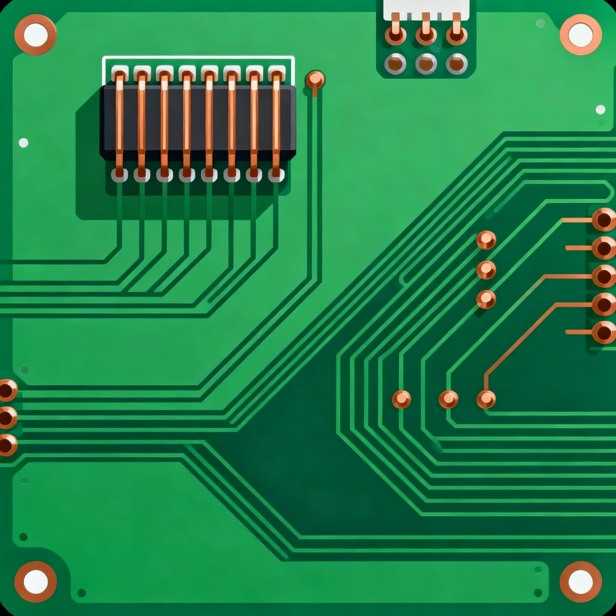
Step-by-Step Design Tutorial for Automotive PCB Assembly: Creating a Vibration-Resistant 4-Layer Board with Press-Fit Connectors
Automotive electronics face a brutal combination of continuous vibration, thermal shock, and contamination. When an engine control unit (ECU) or transmission sensor module must survive 20 g of random ...
Automotive electronics face a brutal combination of continuous vibration, thermal shock, and contamination. When an engine control unit (ECU) or transmission sensor module must survive 20 g of random vibration and temperature swings from −40 °C to +150 °C, the PCB assembly becomes the critical reliability link. This tutorial walks you through designing a vibration-resistant 4‑layer board using press‑fit connectors—a proven architecture that eliminates solder joint fatigue and delivers field lifetimes exceeding 15 years. We’ll cover stackup selection, footprint design, routing techniques, and validation testing, drawing on real‑world failure analysis and industry best practices.
When a 4-Layer Board Must Survive 20 g of Vibration: The Automotive Reality
Under‑hood and chassis‑mounted electronics operate in one of the harshest environments in engineering. Random vibration profiles often exceed 10 grms, with peaks above 20 g, while thermal cycling swings from −40 °C cold‑soak to +150 °C near the exhaust manifold. Add humidity, salt spray, and chemical exposure, and you have a recipe for intermittent failures that no amount of conformal coating alone can solve.
The dominant failure mechanism in conventional soldered assemblies is solder joint fatigue. Differential thermal expansion between the PCB, component leads, and connector pins creates shear stresses that eventually crack the solder fillet. Under vibration, those micro‑cracks propagate rapidly, leading to open circuits or high‑resistance contacts. ALLPCB’s vibration failure analysis documents how cracked solder joints and pad cratering account for over 60% of field returns in transportation electronics. Similarly, PCBgogo’s automotive assembly guide stresses that consumer‑grade PCBs simply cannot absorb the constant mechanical energy present in a vehicle.
A 4‑layer board with press‑fit connectors addresses these risks at the architectural level. The buried ground and power planes add mass and stiffness, raising the board’s natural frequency above the excitation range of most engine harmonics. Press‑fit compliant pins, inserted into plated through‑holes, form a gas‑tight cold weld that does not depend on solder for mechanical or electrical integrity. This combination has become the first line of defense for ECUs, ABS controllers, and battery management systems. Moreover, automotive PCB assembly must operate within a quality management framework such as IATF 16949, as detailed by PCBSync’s automotive PCB guide, which mandates strict process control, traceability, and zero‑defect targets.
How Press-Fit Connectors and Stackup Design Tame Vibration at the Board Level
Vibration energy enters a PCB through its mounting points and travels as bending waves. The board’s dynamic response depends on its stiffness, mass distribution, and boundary conditions. A symmetric 4‑layer stackup—typically arranged as signal‑ground‑power‑signal—provides a substantial increase in bending stiffness compared to a 2‑layer board of the same thickness. The solid copper planes act as constrained layers that dampen high‑frequency modes and spread heat, reducing hot spots that accelerate creep fatigue.
Press‑fit technology eliminates the weakest link: the solder interface. A compliant pin, often with an eye‑of‑needle geometry, deforms elastically as it is pressed into a plated through‑hole. The resulting contact pressure (typically 50–150 N per pin) creates a cold‑welded, gas‑tight junction that is immune to tin whiskers and thermal fatigue. Because there is no solder fillet, the connection can withstand millions of vibration cycles without fretting corrosion. ALLPCB’s vibration isolation analysis highlights how compliant‑pin interconnects shift the failure point away from the connector‑board interface, while PCBCool’s stackup considerations reinforce the importance of symmetric copper distribution to prevent warpage during reflow and press‑fit insertion.
Table 1 – Press‑Fit vs. Soldered Connectors: Key Performance Parameters
| Parameter | Press‑Fit (Compliant Pin) | Soldered (SMT / Through‑Hole) | Notes |
|---|---|---|---|
| Insertion force per pin | 30–80 N (typical) | 0 N (solder reflow) | Requires stiff backup tooling for press‑fit |
| Vibration resistance (sinusoidal) | >20 g, 10–2000 Hz | 10–15 g before solder cracking | Press‑fit cold weld avoids fatigue |
| Shock resistance | >50 g, 11 ms half‑sine | 30–50 g; risk of pad cratering | Press‑fit pin mass is lower |
| Thermal cycling endurance (−40/+150 °C) | >2000 cycles | 500–1000 cycles typical | No CTE mismatch in solder joint |
| Contact resistance stability | <1 mΩ change over life | Can increase due to intermetallic growth | Gas‑tight interface resists oxidation |
| Reworkability | Limited (pin replacement possible) | Easy with hot‑air rework | Press‑fit holes may require new PCB if damaged |
| Tin whisker risk | None (no tin plating on pin) | Present if pure tin finish used | Press‑fit pins typically Ni/Au or SnPb over Ni |
| Typical field failure rate (FIT) | <0.5 FIT per pin | 1–5 FIT per solder joint | Based on automotive telemetry data |
The table underscores why press‑fit has become the default for high‑reliability automotive connectors. The elimination of solder removes the primary fatigue site, while the controlled insertion process guarantees consistent contact force. However, the board design must accommodate the high insertion forces without flexing, which brings us to the stackup and layout rules.
Press-Fit vs. Soldered Connectors: Which One Keeps Your Automotive PCB Alive Longer?
Choosing between press‑fit and soldered terminations is not just a connector decision—it dictates the entire assembly process and long‑term failure signature. MyEMSSolutions’ high‑vibration design guide notes that soldered joints fail predominantly by thermal fatigue and tin whisker growth, while press‑fit connections suffer from fretting only if the pin‑to‑hole interference is lost. PCBSync’s overview of SMT assembly challenges adds that mixed‑technology boards require careful sequencing to avoid damaging compliant pins during reflow.
Table 2 – Failure Modes and Selection Criteria: Press‑Fit vs. Soldered
| Comparison Metric | Press‑Fit Connector (Option A) | Soldered Connector (Option B) | Selection Criteria & Failure Boundary |
|---|---|---|---|
| Primary vibration failure mode | Fretting corrosion if hole plating wears | Solder fatigue cracking at heel/toe | Choose press‑fit when vibration >10 grms; soldered acceptable for cabin modules |
| Susceptibility to tin whiskers | None (compliant pin uses non‑tin finish) | High if pure tin plating; mitigated by Ni/Au or conformal coat | Press‑fit eliminates whisker risk without coating |
| Assembly process complexity | Requires press‑fit machine, backup tooling, post‑solder insertion | Standard SMT reflow or wave solder | Press‑fit adds a secondary operation but removes solder inspection |
| Rework cycle limit | 1–2 re‑insertions before hole damage | 3–5 rework cycles with proper pad repair | Design for no rework; use replaceable connector modules if needed |
| Long‑term contact resistance drift | <2 mΩ over 15 years | 5–20 mΩ due to intermetallic growth | Critical for sensor signal integrity; press‑fit preferred |
| Engine‑mounted ECU suitability | Excellent; survives 20 g and thermal shock | Marginal; requires underfill and massive solder fillets | Press‑fit is the standard for powertrain ECUs |
| Cost per I/O (high‑volume) | $0.02–0.05 per pin (connector + insertion) | $0.01–0.03 per pin (solder + inspection) | Press‑fit premium offset by zero field failures |
In practice, many automotive designs mix both technologies. A board may carry soldered SMT components and press‑fit connectors. The key is to sequence assembly so that reflow soldering is completed first, followed by press‑fit insertion. This prevents thermal damage to the compliant pins and avoids solder re‑melting that could compromise the cold weld. Selective wave soldering may still be needed for through‑hole soldered parts, but the board must be designed to withstand the localized thermal stress without warping the press‑fit holes.
Step-by-Step: Laying Out a Vibration-Proof 4-Layer Board with Press-Fit Terminations
This section provides a practical workflow you can apply to your next ECU or sensor module design. Each step incorporates lessons learned from field failures and the design recommendations of PCBCool’s automotive tutorial and ALLPCB’s vibration damping techniques.
Step 1: Define the 4‑Layer Stackup for Maximum Stiffness
Start with a symmetric stackup that places the ground and power planes on the inner layers. This not only improves signal integrity but also adds mass and flexural rigidity. Use a high‑Tg FR‑4 laminate (Tg ≥ 170 °C) with a low coefficient of thermal expansion (CTE) in the Z‑axis to minimize barrel cracking during thermal cycling. The total board thickness should be at least 1.6 mm; for engine‑mounted modules, 2.0 mm or thicker is common.
Table 3 – Recommended 4‑Layer Stackup for Vibration‑Resistant Automotive PCB
| Layer | Material / Thickness | Function | Notes |
|---|---|---|---|
| Top (L1) | 1 oz Cu, plated to 1.5 oz after plating | Signal + component pads | Use teardrops on all pads; avoid acute angles |
| Prepreg | 1080 (2.8 mil) or 2116 (4.5 mil) | Dielectric | Low‑flow prepreg for press‑fit hole stability |
| Inner 1 (L2) | 1 oz Cu (solid plane) | Ground plane | Continuous plane; no splits under connectors |
| Core | 0.8 mm (31 mil) high‑Tg FR‑4 | Substrate | Tg 170–180 °C, Z‑CTE < 3.5% |
| Inner 2 (L3) | 1 oz Cu (solid plane) | Power plane | May be split for multiple voltages; keep copper balanced |
| Prepreg | 2116 (4.5 mil) or 2×1080 | Dielectric | Symmetrical to top prepreg for flatness |
| Bottom (L4) | 1 oz Cu, plated to 1.5 oz | Signal + connector pads | Mirror top layer copper pour for symmetry |
| Total thickness | 1.6 mm ±10% | – | Adjust core/prepreg to meet target |
This stackup yields a first natural frequency above 200 Hz when properly mounted, well above the 50–150 Hz range of most engine vibrations. Always verify with a modal analysis using your CAD tool’s FEA module or a dedicated simulation package.
Step 2: Place Heavy Components and Connectors Near Mounting Points
Components with significant mass—large electrolytic capacitors, inductors, and press‑fit connectors—should be placed as close as possible to the board’s mounting holes. This reduces the lever arm that amplifies acceleration forces. Avoid placing tall connectors at the board edge where bending moment is highest. If edge placement is unavoidable, add additional mounting screws or stiffening ribs.
Step 3: Design Press‑Fit Connector Footprints to Manufacturer Specifications
Press‑fit holes require tighter tolerances than standard PTH. The finished hole diameter must match the connector vendor’s recommended range, typically with a tolerance of ±0.05 mm. The hole wall must be free of burrs and have a uniform copper plating thickness (25–35 µm). Annular rings should be at least 0.25 mm to provide a stable landing for the pin shoulder. Never use solder mask in the press‑fit area; it can contaminate the contact zone. Download the connector manufacturer’s PCB footprint guidelines and follow them exactly—deviations are the leading cause of insertion force problems and intermittent contacts.
Step 4: Route with Teardrops and Anchor Pads for Strain Relief
Every pad and via connected to a press‑fit hole or a heavy component should include a teardrop (filleted trace entry). Teardrops distribute stress and prevent trace cracking at the pad interface. For SMT components near connectors, use anchor pads (extra copper extensions) to increase adhesion. Route high‑speed signals on the top layer with immediate via transitions to inner layers to minimize stub lengths. Keep traces away from board edges by at least 3 mm to avoid delamination during vibration.
Step 5: Reinforce Mounting Holes
Mounting holes should be plated and surrounded by a generous annular ring (≥1 mm) tied to the ground plane with multiple vias. This creates a robust mechanical anchor and a low‑impedance path to chassis ground. Use a star‑washer or serrated screw head to ensure a gas‑tight connection to the enclosure. For boards thicker than 1.6 mm, consider adding a metal stiffener bracket bonded to the PCB with thermally conductive adhesive.
Step 6: Validate Against IEC 60068‑2‑6 Vibration Profiles
Before releasing the design to production, subject prototypes to swept‑sine and random vibration tests per IEC 60068‑2‑6. Typical automotive profiles include 10–2000 Hz at 2 g acceleration for cabin electronics, and 20–2000 Hz at 5 g for engine‑mounted modules. Monitor contact resistance in‑situ using a daisy‑chain test vehicle that includes the press‑fit connectors. Look for any resistance spikes exceeding 1 µs in duration. Post‑test, perform cross‑section analysis of press‑fit holes to verify the cold weld and check for barrel cracks.
Tip: Work with your PCB fabricator to qualify the laminate for CAF (conductive anodic filament) resistance. Automotive environments with high humidity and bias voltage can cause CAF growth between adjacent vias, leading to field failures that are almost impossible to detect during functional test.
What Automotive PCB Designers Ask About Vibration-Resistant Assemblies
Q: What IPC performance class should I specify for a vibration-resistant automotive PCB?
A: Class 2 is the baseline for most automotive electronics, covering infotainment, body controls, and comfort modules. However, mission‑critical systems—powertrain, braking, steering, and advanced driver‑assistance systems (ADAS)—demand Class 3 to ensure higher reliability under vibration and thermal cycling. Class 3 imposes tighter requirements on plating thickness (≥25 µm in holes), annular ring breakout (no more than 90°), and inspection criteria. PCBSync’s certification insights note that many Tier 1 suppliers default to Class 3 for any module that could affect vehicle safety, even if the OEM specification only calls for Class 2.
Q: Can a 4-layer board provide enough rigidity for an engine-mounted ECU?
A: Yes, when designed with a symmetric stackup, high‑Tg FR‑4, and adequate mounting points. The key is controlling board thickness (typically 1.6 mm or more) and using press‑fit connectors that don’t rely on solder fillets for mechanical strength. A 4‑layer board with solid inner planes has significantly higher bending stiffness than a 2‑layer board of the same thickness. Finite element analysis or physical vibration testing is recommended to verify the design. In extreme cases (e.g., direct engine block mounting), you may need to increase thickness to 2.0 mm or add a metal stiffener, but a properly executed 4‑layer stackup is sufficient for most under‑hood ECUs.
Q: How do I validate press-fit connector reliability without soldering?
A: Validation relies on cross‑section analysis to verify the gas‑tight cold weld, pin‑retention force measurements (typically >50 N per pin after insertion), and accelerated life testing under combined vibration and thermal cycling (e.g., IEC 60068‑2‑6 and IEC 60068‑2‑14). Many connector vendors provide qualification reports that can be supplemented with in‑house testing on the actual PCB stackup. A common practice is to build a dedicated test coupon with daisy‑chained press‑fit pins and monitor resistance continuously during 1000 thermal cycles and 24 hours of random vibration. Any resistance shift >1 mΩ warrants a root‑cause investigation.
Q: Are there lead‑time risks when sourcing high‑Tg FR‑4 for automotive builds?
A: High‑Tg materials like Isola 370HR or Shengyi S1000‑2 are widely available, but supply can tighten during industry upswings. It’s wise to qualify an alternate laminate with equivalent IPC‑4101 slash sheets and to keep buffer stock for long‑running programs, especially if the board requires UL 94 V‑0 and CAF resistance. MyEMSSolutions’ design considerations emphasize that locking in a single laminate source without an approved second source is a common supply‑chain mistake that can delay production by 8–12 weeks.
Q: Can I mix press‑fit and soldered components on the same board?
A: Yes, but the assembly sequence matters. Press‑fit connectors are usually inserted after reflow soldering to avoid thermal damage to the compliant pins. The board must be designed so that press‑fit forces don’t stress nearby SMT joints—place press‑fit connectors at least 5 mm away from small chip components and avoid placing them on the opposite side of thin boards. Selective wave soldering may be needed if through‑hole soldered parts are also present, and the board must be supported to prevent flexing during the press‑fit operation. A well‑designed assembly fixture that backs up the board directly under the connector is essential.
References & Further Reading
- Vibration Resistance in Transportation PCBs – ALLPCB
- Vibration Analysis of Electronic PCB Components – ALLPCB
- Automotive PCB Design Tutorial for Real-World Conditions – PCBCool
- Automotive PCB: Design, SMT Assembly & Quality Standards – PCBSync
- What is Automotive PCB Assembly? – PCBgogo
- Designing PCBs to Withstand High Vibration Applications – MyEMSSolutions
- Press‑Fit Connector Technology – TE Connectivity
- Automotive PCB Assembly Services – NovaPCBA
Conclusion: Designing a vibration‑resistant 4‑layer board with press‑fit connectors is a multi‑disciplinary exercise that blends material science, mechanical engineering, and precision assembly. By following the stackup, layout, and validation steps outlined here, you can build ECUs and sensor modules that survive 20 g of vibration and decades of thermal cycling without a single solder joint failure. At NovaPCBA, we support automotive Tier 1 and OEM customers with IATF 16949‑certified assembly lines, press‑fit insertion capability, and in‑house vibration testing to help you move from prototype to production with confidence. When reliability is non‑negotiable, the right board architecture and a trusted manufacturing partner make all the difference.