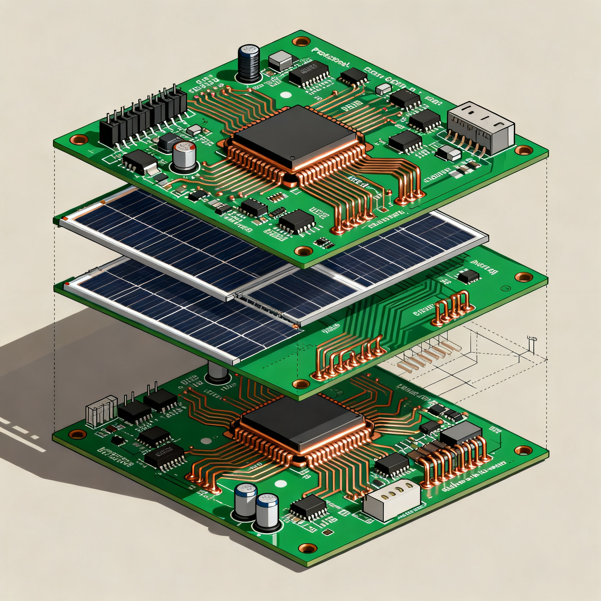
Step-by-Step Design Tutorial for 4-Layer Heavy Copper Energy PCB Assembly in Solar Inverters
Why Solar Inverter Designers Are Rethinking PCB Copper—and Stackup If you’ve ever had to re-spin a solar inverter power board because a buried inner‑layer short didn’t show up until the final 300 V te...
Why Solar Inverter Designers Are Rethinking PCB Copper—and Stackup
If you’ve ever had to re-spin a solar inverter power board because a buried inner‑layer short didn’t show up until the final 300 V test, you already know the pain. Unlike low‑voltage logic boards, a solar inverter’s continuous 30 A to 80 A bus currents, combined with daily thermal swings from -40 °C to +85 °C, turn ordinary FR‑4 into a ticking time bomb. The culprit is often invisible: inner layer defects that form during etching and become completely unreachable after lamination. As BestPCBs notes, automated optical inspection (AOI) of inner layers is critical because once those layers are pressed, no rework is possible.
That’s why seasoned energy product teams are moving away from thin 1 oz copper inner layers and embracing a 4‑layer heavy copper stackup. The change isn’t just about handling more amps; it’s about building a board that stays thermally stable and electrically quiet for the 15‑year lifetime of a rooftop inverter. Adding substantial copper mass on the inner planes directly attacks two problems: heat concentration and conducted EMI. As MorePCB’s design guide explains, additional copper layers help dissipate heat more effectively, keeping components cooler and improving reliability. And when you’re switching 600 V IGBTs or SiC MOSFETs at 20 kHz, the low‑impedance return paths provided by a 4‑layer stackup (with dedicated power and ground planes) dramatically reduce ringing and EMI, as detailed in Aivon’s comprehensive 4‑layer design guide.
The real question isn’t “should I use a 4‑layer board?” but “how do I design a 4‑layer heavy copper board that won’t delaminate, warp, or fail DFM?” That’s the step‑by‑step journey we’ll walk through in this tutorial, from stackup selection to Gerber verification, all with the specific needs of a 2 kW–5 kW solar inverter in mind.
The Nuts and Bolts of a 4-Layer Heavy Copper Stackup for High-Current Energy Paths
Before you place a single component, you need to lock down the stackup. A 4‑layer heavy copper board for a solar inverter typically uses a symmetrical construction: a thick core with two inner layers, prepreg bonding sheets, and then two outer layers. The copper weights you choose will define not only current capacity but also the board’s thermal and mechanical behavior.
Common copper thicknesses for heavy copper designs range from 2 oz to 6 oz per layer. BestPCBs recommends that for a custom 4‑layer heavy copper PCB, outer layers often carry 3 oz or 4 oz, while inner layers can be 2 oz to 4 oz depending on the current path. In a typical solar inverter, you might use 4 oz on the outer layers for the DC bus and phase outputs, and 3 oz on the inner power plane to keep the stackup symmetrical and reduce delamination risk.
The table below gives a practical starting stackup for a 2 kW inverter with 40 A continuous bus current. All values are based on IPC‑2221 trace width calculations for a 10 °C temperature rise.
| Layer | Material / Copper Weight | Typical Use | Key Constraint |
|---|---|---|---|
| Top (L1) | 4 oz Cu foil + plating | DC+ bus, IGBT drains, high‑current connectors | Min. trace width 2.5 mm for 40 A |
| Prepreg | 2× 1080 + 1× 2116 (high resin content) | Bonding and gap fill | Resin‑rich to flow into thick copper features |
| L2 – Inner Power Plane | 3 oz Cu (0.5 oz base + 2.5 oz plated) | GND plane, return currents, secondary rail islands | 20% copper balance vs. L3; island shapes for localized rails |
| Core | 0.2 mm FR‑4 High‑Tg (170 °C) | Mechanical backbone | Stable thickness for impedance control |
| L3 – Inner Power Plane | 3 oz Cu | Split power plane (e.g., +15 V, +5 V analog) | Use localized islands, not wide splits; maintain balance |
| Prepreg | 2× 1080 + 1× 2116 | Bonding | Same as above |
| Bottom (L4) | 4 oz Cu | Phase outputs, shunt resistors, gate drive traces | Keep gate traces short; avoid crossing high‑dV/dt nodes |
Tip: Notice that the inner layers are slightly lighter than the outer layers. This is deliberate. Outer layers benefit from additional plating, which can push the effective copper thickness to 4 oz or more, while inner layers at 3 oz provide enough cross‑sectional area for 80 A continuous loads when using wide pours and multiple via arrays. The copper balance between L2 and L3 must be maintained within ±20% to avoid lamination stress, as JHYPCB’s design guidelines emphasize. If you need a secondary rail like +5 V for the microcontroller, create a localized island on L3 connected by a wide trace and bus vias, not a huge split across the plane, to keep the copper distribution even.
Current carrying capacity is calculated using IPC‑2221 charts. For an outer layer at 4 oz, a trace width of approximately 40 mm is required for 80 A at a 10 °C rise. On an inner layer at 3 oz, a 60 mm wide pour or a combination of parallel traces and stitching vias can handle the same current. Aivon’s heavy copper design guide provides a full set of thermal management strategies, including the use of thermal vias under power semiconductors and the importance of keeping copper pours continuous to avoid hot spots. For a solar inverter, the DC link capacitor bank and the IGBT module are the hottest zones; place thermal reliefs only where absolutely necessary for soldering, and use a solid connection for the main current path.
Key Takeaways: Choose copper weights that match your continuous current, not just peak. Maintain copper balance. Plan for resin‑rich prepreg to fill the gaps between thick copper features. And always verify your stackup with your manufacturer’s engineering team before releasing the Gerber files.
Heavy Copper 4-Layer vs. Standard 4-Layer: When the Extra Cost Translates to Inverter Reliability
Deciding between a standard 4‑layer board (1 oz copper throughout) and a heavy copper 4‑layer build (3 oz–4 oz) is, at its core, a trade‑off between upfront unit cost and long‑term field reliability. The table below compares the two approaches for a 2 kW solar inverter with a 40 A continuous bus, using data from real manufacturing sources and industry practices.
| Comparison Metric | Standard 4‑Layer (1 oz) PCB | Heavy Copper 4‑Layer (4 oz outer / 3 oz inner) | Selection Criteria & Failure Boundary |
|---|---|---|---|
| Conductor cross‑sectional area (outer layer) | 35 µm (1 oz) | 140 µm (4 oz) | For 40 A, 1 oz requires trace width ~22 mm; 4 oz only ~8 mm. Board real‑estate savings offset cost. |
| Thermal resistance (junction‑to‑ambient, typical) | High; copper acts as a heat spreader but limited mass | Low; 4× copper mass reduces hotspot temperature 10–15 °C | If ambient reaches 70 °C, 1 oz may push IGBT junction near 150 °C; 4 oz keeps it under 135 °C. |
| Delamination risk under thermal cycling | Low; thin copper and low CTE mismatch | Moderate; requires high‑Tg FR‑4, resin‑rich prepreg, and copper balance | Without 20% balance, inner layers can separate after 1000 cycles. Critical for -40 °C to +85 °C operation. |
| Unit cost (prototype, 1000 × 150 mm) | $8–$12 | $15–$25 | Heavy copper adds 30–60% to unit cost. PCBSync notes the gap has narrowed; overseas manufacturers offer 4‑layer prototypes approaching 2‑layer prices. |
| Rush service premium | 1.5–2× standard lead time | 2–3× standard lead time, 7–10 days typical | Wonderful PCB warns that rush service for heavy copper costs 2–3× more; avoid unless for a trade show demo. |
| Current handling at 10 A, 30 A, and 80 A continuous | 10 A: 5 mm trace; 30 A: 15 mm; 80 A: not practical without external busbars | 10 A: 1.5 mm; 30 A: 4 mm; 80 A: 40 mm outer, 60 mm inner with vias | Above 80 A and 4 oz, current path rules from BestPCBs recommend parallel paths and thermal reliefs on vias. |
The cost premium of heavy copper is real, and it’s easy to get sticker shock on the first prototype order. But when you amortize that added cost over the expected 15‑year service life of a solar inverter, the math shifts. A single field failure due to a burned‑out trace on a 1 oz board can wipe out the savings of a thousand units. The threshold where heavy copper becomes mandatory is around 20 A continuous in a confined space. Once you exceed 30 A, the thermal runaway risk on a 1 oz inner layer is too high, as Aivon’s thermal analysis shows. For a 2 kW inverter, a 4‑layer heavy copper board is not an over‑engineered luxury; it’s an insurance policy against latent inner‑layer defects.
If your design is a low‑power microinverter (300 W) with a 10 A bus, a standard 4‑layer board may suffice. But for string inverters in the 2 kW–5 kW range, the heavy copper stackup is the default choice among experienced design teams. And when you need prototype boards quickly, plan for a 7–10‑day lead time and a 40–60% cost premium over standard 4‑layer, as highlighted by Wonderful PCB. Overnight services exist but are exponentially more expensive, so they are best reserved for true emergencies.
A Step-by-Step Walkthrough: From Schematic to Gerber for a 4-Layer Heavy Copper Solar Inverter Board
Designing a heavy copper board for a solar inverter isn’t fundamentally different from a standard PCB, but the devil is in the details of the stackup and the DFM constraints. This walkthrough assumes you’re using a CAD tool like Altium Designer, KiCad, or Cadence Allegro, and that you’re targeting a 2 kW inverter with a 40 A continuous DC bus, 400 V DC link, and a single‑phase AC output.
Step 1: Schematic Capture and Component Selection
Start with a clear power topology: DC input filter → boost converter (if needed) → DC link capacitors → full‑bridge IGBT module → output filter. For each high‑current net, define the expected DC and peak ripple current. Use footprints with large copper pads for power components—TO‑247, SOT‑227, and large SMD shunt resistors. Avoid QFN packages in the main power path; they lack the pad area needed for heavy copper soldering. Assign net classes for the power nets with a minimum trace width of 4 mm (for 4 oz outer) and clearance of 0.3 mm.
Step 2: Stackup Definition and Layer Assignment
Using the stackup from Section 2, define your layers in the CAD tool. Outer layers (L1 and L4) carry the high‑current switched paths—keep the DC+ and phase output traces as wide and short as possible. L2 is a solid GND plane; L3 is a split power plane for the low‑voltage control circuitry (+15 V, +5 V). JHYPCB’s guidelines advise using localized islands for secondary rails on L3, connected to the main ground through wide traces and bus vias. This prevents the lamination stress that would occur if you tried to maintain a large split across the whole plane while keeping copper balance.
Step 3: Via Placement and Current Sharing
For a 40 A bus, you’ll need multiple vias in parallel. A single 0.3 mm hole with 4 oz plating can carry about 3 A; for 40 A you need at least 14 vias. Place them in a grid under the IGBT module’s drain pad and near the DC link capacitor terminals. Use teardrops on all heavy copper pads to reduce stress concentration, as recommended by Aivon’s heavy copper guide.
Step 4: Copper Balancing and Thermal Relief
Before pouring copper planes, check the copper coverage on each layer. The difference between L2 and L3 should be less than 20%. If your control circuitry requires only a small island, fill the remaining area of L3 with a copper pour connected to GND (or a dummy net) to maintain balance. This is a non‑negotiable rule for heavy copper boards; ignoring it is the most common cause of lamination warpage and inner‑layer delamination, as JHYPCB and many fabricators have documented. For the thermal reliefs on through‑hole pads of connectors and large capacitors, use a 4‑spoke pattern with 0.5 mm web width—enough to reduce heat sinking during soldering but not so thin as to create a current bottleneck.
Step 5: DFM Review and Gerber Verification
Before sending out the files, run a rigorous DFM check. BestPCBs’ engineering review process includes checking trace width, spacing, annular ring, and copper balance. Pay special attention to inner layer annular rings. For a 0.5 mm via, the annular ring should be at least 0.2 mm with heavy copper, because the plating process can cause small variations. A breakout on an inner layer will not be caught until the board is built and fails hipot testing. Also, verify that all inner layer clearances are respected; AOI inspection after etching is the only chance to catch shorts and opens, as BestPCBs notes, because lamination makes those defects permanent.
Generate Gerber RS‑274X files and export the NC drill file. Include a detailed fabrication drawing that specifies the stackup, material type (high‑Tg FR‑4, 170 °C), copper weights, and any impedance control requirements if you have fast‑switching gate drive signals. Weller PCB’s heavy copper manufacturing guide provides a checklist of what to include in your fabrication notes to avoid delays.
The entire design flow—from schematic to Gerber release—can be summarized in a table that mirrors the typical 4‑layer design guide steps from MorePCB, adapted for heavy copper.
| Design Phase | Action | Heavy Copper Specifics | Verification |
|---|---|---|---|
| 1. Schematic | Define net classes, current ratings, and component footprints | Set power net class to 4 mm min width, 0.3 mm clearance | ERC run; check for missing power flags |
| 2. Stackup | Configure layer stack, copper weights, and materials | 4 oz outer, 3 oz inner, high‑Tg FR‑4, resin‑rich prepreg | Cross‑check with fabricator’s capabilities |
| 3. Placement | Place power components, gate drivers, and connectors | Keep high‑current loops tight; avoid daisy‑chaining ground | 3D clearance check; thermal simulation |
| 4. Routing | Route power traces and planes, add vias | Use wide pours, parallel vias, teardrops; solid connections for power | DRC on all layers; check via count |
| 5. Copper Balancing | Pour dummy copper on sparse layers | Maintain ±20% between L2 and L3; use localized islands | Layer‑by‑layer copper coverage report |
| 6. DFM & Gerber | Run DFM checks, generate Gerber, and add fab notes | Check annular rings, inner layer clearances, and AOI readiness | Gerber viewer; supply stackup drawing |
Following this sequence, and collaborating early with your PCB manufacturer, will dramatically reduce the risk of inner‑layer shorts, warpage, and field failures. At NovaPCBA, our assembly line for heavy copper boards is optimized for the thick copper and high thermal mass of solar inverter designs, and our engineering team routinely reviews stackups and DFM files to catch issues before they become prototypes. When you’re ready to move from CAD to a real board, reaching out early ensures that the manufacturer’s capabilities align with your design intent.
Questions from the Field: Solar Inverter PCB Design Teams on Heavy Copper Decisions
Q: What copper weight do I need for an 80 A continuous bus in a solar inverter?
For an 80 A continuous load, outer layer copper at 4 oz requires a trace width of approximately 40 mm based on IPC‑2221 for a 10 °C temperature rise. This is typically achieved by a wide polygon pour, not a single thin trace. On an inner layer at 3 oz, you can handle 80 A with a 60 mm wide pour combined with multiple via arrays that stitch the current to the outer layers. The key is to use multiple parallel vias—at least 25–30 vias of 0.5 mm diameter—to distribute the current from the inner plane to the outer layer pads. Thermal reliefs on these vias should be minimal or omitted for the main current path to avoid bottlenecks.
Q: How do I prevent delamination when using 4 oz copper on inner layers?
Delamination is a real risk when thick copper layers are combined with resin‑starved prepreg. To prevent it, maintain copper balance within ±20% between all layers, especially L2 and L3. Use teardrops on all heavy copper pads and vias to reduce mechanical stress. Specify a high‑Tg FR‑4 laminate (170 °C minimum) and ask your fabricator to use resin‑rich prepreg sheets (e.g., two layers of 1080 with a 2116) to ensure the resin flows into the gaps between thick copper features. Avoid abrupt transitions from 4 oz traces to thin signal traces; taper the width gradually over at least 2 mm. Finally, ensure your layout includes a solid copper border around the board edge to act as a mechanical anchor.
Q: Can I expect a 4-layer heavy copper prototype in under 5 days? What’s the cost premium?
A 5‑day turnaround for a heavy copper 4‑layer prototype is very aggressive and usually not offered as a standard service. According to Wonderful PCB, rush service for heavy copper boards typically costs 2–3× the standard lead time price. Expect a realistic fast‑turn time of 7–10 working days, with a 40–60% premium over the standard 4‑layer price. If you need boards in under 5 days, you are looking at a super‑rush service that can push the cost to 3–5× the standard price, and availability depends heavily on the factory’s current workload. Unless you are racing to a critical trade show demo, it’s far more economical to plan for 10‑day lead times.
Q: What is the most overlooked DFM rule for heavy copper inner layers?
Without question, it’s the failure to catch inner layer defects before lamination. BestPCBs highlights that automated optical inspection (AOI) after inner layer etching is the only chance to find shorts, opens, and copper residue. Once the layers are pressed, those defects are sealed in forever. Another frequently overlooked rule is ensuring sufficient annular ring on large vias. With heavy copper, plating thickness can vary, and a small annular ring can lead to breakout. A minimum annular ring of 0.25 mm for vias over 0.4 mm diameter is recommended. Also, always check that the inner layer clearances are large enough for the copper weight—a 0.2 mm clearance may be fine for 1 oz but is likely to be etched away or cause shorts on 3 oz copper.
Q: Is it better to use a single 4-layer heavy copper board or a separate power board with busbars?
The answer depends on the current level. For currents up to about 100 A, a single 4‑layer heavy copper PCB integrates both the power paths and the control circuitry on one board, which reduces assembly steps, eliminates inter‑board connectors, and lowers parasitic inductance—a critical advantage when switching at high speeds. For currents above 200 A, the required copper weight and trace width become impractical; at that point, a separate power board with laminated busbars and a control board is more cost‑effective. In the 30–100 A range typical of residential string inverters, a well‑designed 4‑layer heavy copper board is the sweet spot, offering a compact, reliable solution that’s easier to manufacture and test.
Q: How do I handle thermal expansion mismatch in a solar inverter that cycles from -40 °C to +85 °C?
The wide temperature swing of an outdoor solar inverter puts enormous strain on the PCB. Copper’s coefficient of thermal expansion (CTE) is about 17 ppm/°C, while FR‑4 is 14–16 ppm/°C in the x‑y direction and much higher in the z‑axis. With 4 oz copper, the mismatch can cause plated through‑hole cracking. To mitigate this, use a high‑Tg FR‑4 (170 °C) with a low CTE, and if possible, limit inner layer copper to 4 oz or less. Add strain relief slots around large heatsinks and heavy components. Simulation of thermal cycling according to IPC‑TM‑650 and compliance with IPC‑6012 Class 3 for heavy copper are recommended to validate the design. Incorporating a few redundant vias and avoiding sharp corners on copper pours also helps distribute stress.
References & Further Reading
- Custom 4‑Layer Heavy Copper PCB Manufacturer for High‑Current Power Applications – BestPCBs
- How to Design 4 Layer PCB: Complete Step‑by‑Step Guide – MorePCB
- Mastering 4‑Layer PCB Design: A Comprehensive Guide to Layout & Stackup – Aivon
- 4 Layer PCB Design Guidelines: From Stackup Planning to DFM – JHYPCB
- 4 Layer PCB: Complete Guide to Stackup, Design & Manufacturing – PCBSync
- Heavy Copper PCB Design: Principles, Rules, and Best Practices – Aivon
- 4‑Layer PCB Manufacturing and Stack‑up – Wonderful PCB
- Heavy Copper PCB Manufacturing: Design Rules, Applications & Process Guide – Weller PCB