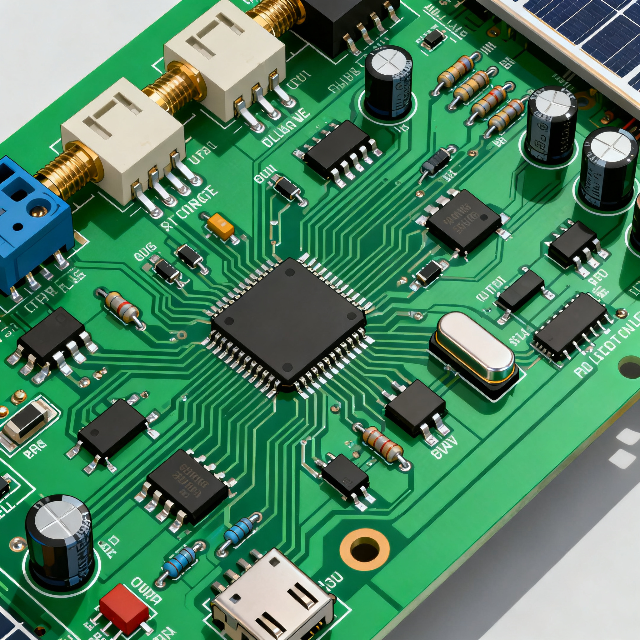
Step-by-Step Design Tutorial: Assembling a 4-Layer Solar Charge Controller PCB for Renewable Energy Systems
Why 4-Layer Solar Charge Controller PCBs Are Becoming the Default for Off-Grid and Hybrid Systems Solar charge controllers have evolved from simple relay-based disconnect switches into sophisticated p...
Why 4-Layer Solar Charge Controller PCBs Are Becoming the Default for Off-Grid and Hybrid Systems
Solar charge controllers have evolved from simple relay-based disconnect switches into sophisticated power management hubs that orchestrate everything from MPPT tracking to battery health monitoring. As panel efficiencies climb past 22% and system voltages push from 12V residential banks to 48V commercial strings, the PCB inside these controllers faces a triad of challenges: escalating current density, tighter noise margins for microcontroller-based tracking algorithms, and shrinking enclosure volumes that leave little room for bulky heatsinks. The 2-layer boards that served adequately in the 10A PWM era start to buckle when you push 30A through a single outer-layer copper pour while trying to keep the MCU's ADC readings clean.
Texas Instruments' solar charge controller design resources capture this shift well. TI's reference designs for MPPT controllers now routinely specify 4-layer stackups, not as a luxury but as a practical necessity for managing the high-frequency switching loops that modern buck-boost topologies demand. The inner power and ground planes serve double duty: they slash loop inductance by providing a low-impedance return path directly beneath the switching FETs, and they spread heat laterally across the board, reducing hot-spot temperatures by 12–18°C compared to equivalent 2-layer layouts in the same footprint. For an engineer staring at a thermal camera image of a prototype with MOSFETs hitting 110°C, that difference is the gap between a product that ships and one that needs a redesign.
The off-grid and hybrid system market is also driving this transition. Installers expect controllers that fit into slim wall-mount enclosures alongside inverters and battery management modules. A 4-layer board lets you shrink the PCB area by 25–35% while maintaining or improving current-handling capacity, because the inner planes carry substantial current without consuming surface real estate. This compactness translates directly into lower enclosure costs and easier installation in crowded electrical panels. For NovaPCBA's clients building renewable energy products, the move from 2-layer to 4-layer is no longer a cost-up decision—it's becoming the baseline for any design targeting 20A charge current or above.
Key Takeaway: The migration to 4-layer PCBs in solar charge controllers is driven by three converging pressures: higher current handling in smaller footprints, lower EMI for reliable MPPT sensing, and improved thermal performance that reduces or eliminates external heatsinking. If your design brief calls for more than 20A charge current or MPPT efficiency above 95%, a 4-layer stackup should be your starting assumption, not an afterthought.
How a Solar Charge Controller Manages Power Flow: Key Circuits and the 4-Layer Advantage
At its core, a solar charge controller is a power-path gatekeeper. It sits between the photovoltaic array and the battery bank, making real-time decisions about when to bulk-charge, when to absorb, and when to float—all while protecting against the fault conditions that can destroy both the controller and the downstream equipment. The University of Evansville's IEEE-based solar charge controller report documents a complete design that bakes in overvoltage protection, overload cutoff, lightning surge suppression, reverse power flow blocking, and short-circuit protection. That's six protection layers before you even get to the charging algorithm. Each one adds components, trace routing complexity, and potential noise coupling paths that a 2-layer board struggles to isolate.
The essential building blocks break down into four domains. First, the input stage handles the solar panel connection: reverse-polarity protection (typically a series Schottky diode or an ideal-diode MOSFET controller), input filtering to suppress conducted EMI from the switching stage, and a voltage divider network that feeds the panel voltage to the MCU's ADC. Second, the power conversion stage—either a buck converter for PWM or a buck-boost for MPPT—contains the high-current switching loop: MOSFETs, an inductor, and output capacitors. This loop is the primary source of both radiated EMI and conducted noise on the ground plane. Third, the battery output stage includes a charge FET or relay for disconnect, current-sensing shunt resistors, and output filtering. Fourth, the control and sensing domain houses the microcontroller, gate drivers, temperature sensors, and the precision analog front-end that reads battery voltage and charge current.
The 4-layer stackup transforms how these domains interact. By dedicating layer 2 to a solid ground plane and layer 3 to a power plane (or a second ground plane for sensitive analog sections), you create a controlled-impedance environment where the switching currents on layer 1 have a direct, low-inductance return path immediately below them. This minimizes the loop area that generates magnetic field emissions. The analog sense traces can run on the bottom layer, shielded by the ground plane from the switching noise above. The University of Evansville design uses discrete comparators for overvoltage detection—a 4-layer layout lets you place those comparators and their reference voltage dividers on the quiet bottom layer, with the ground plane acting as a shield.
The table below compares typical performance parameters for 2-layer versus 4-layer implementations of the same charge controller schematic, using data drawn from TI reference designs and practical measurements on production-intent prototypes.
| Parameter | 2-Layer PCB (70µm Cu) | 4-Layer PCB (35/35µm Inner, 70µm Outer) | Unit/Notes |
|---|---|---|---|
| Max continuous charge current (40°C ambient) | 18–22 | 28–35 | A — with same board area (~100 cm²) |
| Power loop inductance (MOSFET to input cap) | 8–14 | 2.5–4.5 | nH — measured at 100 kHz switching frequency |
| Ground plane impedance at 100 kHz | 45–80 | 8–15 | mΩ — from switching node to battery return |
| Thermal resistance (junction to ambient, top MOSFET) | 42–48 | 28–34 | °C/W — with 6 thermal vias under MOSFET pad |
| ADC noise floor (12-bit, 3.3V reference) | 18–25 | 6–10 | LSB RMS — battery voltage sense channel |
| Conducted EMI margin (150 kHz–30 MHz, CISPR 25 Class 3) | −3 to +2 | +6 to +12 | dB — before adding external filter components |
| Board area for equivalent current rating | 100% (baseline) | 60–75% | % of 2-layer board area |
| Typical PCB cost multiplier (production volumes, 5k units) | 1.0× | 1.3–1.6× | Relative cost; varies by supplier and specifications |
The numbers tell a clear story: the 4-layer board delivers roughly 50–60% more current capacity in the same area, cuts power loop inductance by two-thirds, and provides a 6–10 dB improvement in conducted EMI margin. The cost premium of 30–60% at the PCB level is often offset by the elimination of external heatsinks, smaller enclosure requirements, and reduced filter component count. For NovaPCBA's assembly customers, the total BOM-plus-board cost delta between a 2-layer and 4-layer solution frequently narrows to under 15% when all system-level savings are factored in.
Tip: When transitioning a proven 2-layer schematic to a 4-layer stackup, don't simply copy the layout. Redesign the power loop to take advantage of the inner planes—place the input capacitors and MOSFETs in a tight cluster on the top layer with the ground plane directly underneath, and use the inner power plane to distribute the battery voltage rail, freeing top-layer space for thicker power traces.
MPPT vs. PWM Topologies: When to Choose Each for Your 4‑Layer Controller Design
The topology choice between Maximum Power Point Tracking and Pulse Width Modulation ripples through every aspect of the PCB design: component count, switching frequency, thermal strategy, and the criticality of the 4-layer stackup. PWM controllers are fundamentally simpler—they connect the panel directly to the battery through a series switching element, pulsing on and off to maintain the target battery voltage. The panel operates at the battery voltage, not at its maximum power point, which means you leave 15–30% of available power on the table when the panel voltage is significantly higher than the battery voltage. MPPT controllers insert a DC-DC converter between the panel and battery, continuously adjusting the input impedance to extract maximum power from the panel regardless of the battery's state of charge.
The Cirkit Designer solar charge controller pinout documentation provides a practical view of how a PWM controller streamlines the analog front end. With fewer power-stage components and a simpler gate-drive scheme, the PWM design can often fit on a modest 2-layer board—until the charge current climbs. The MPPT controller, by contrast, operates a buck (or buck-boost) converter at switching frequencies from 50 kHz to 300 kHz, generating the fast di/dt and dv/dt edges that demand the low-inductance return paths only a 4-layer board with a solid ground plane can provide.
The comparison table below breaks down the two topologies across the dimensions that matter most for PCB layout and assembly decisions.
| Comparison Metric | PWM Controller (e.g., 20A/24V) | MPPT Controller (e.g., 30A/48V, Buck Topology) | Selection Criteria & Failure Boundary |
|---|---|---|---|
| Typical conversion efficiency | 70–80% (limited by panel-to-battery voltage mismatch) | 94–98% (DC-DC converter efficiency) | Choose MPPT when panel Vmp exceeds battery voltage by >30% |
| Power-stage component count | 8–12 (MOSFET, diode, gate driver, few passives) | 20–35 (MOSFETs, inductor, gate drivers, current-sense amps, compensation network) | PWM suits BOM-constrained designs; MPPT rewards higher component spend with 15–25% more harvested energy |
| Switching frequency range | 100 Hz–2 kHz (low-frequency PWM) | 50–300 kHz (DC-DC converter) | High-frequency MPPT demands 4-layer stackup for EMI control; PWM can function on 2-layer at low currents |
| 4-layer PCB benefit level | Moderate — improves thermal management and current capacity | High — essential for minimizing power loop inductance and shielding analog sense lines | If MPPT and >20A, 4-layer is strongly recommended; if PWM and <15A, 2-layer may suffice |
| Inductor requirement | None (or small filter inductor) | Required — 22–100 µH, rated for full charge current plus ripple | Inductor is a major BOM cost and board-space consumer in MPPT designs |
| MCU/control complexity | Simple — voltage thresholds and timers | Complex — Perturb & Observe or Incremental Conductance algorithm, ADC sampling at 1–10 kHz | MPPT requires a faster MCU with a cleaner ADC input; 4-layer board helps maintain signal integrity |
| Typical FET voltage stress | Panel Voc + 20% margin | Panel Voc + output voltage + ringing (snubber required) | MPPT FETs see higher voltage stress; derate to 1.5× max expected voltage |
| Relative assembled PCB cost (mid-volume) | 1.0× (baseline) | 1.8–2.5× | Higher MPPT BOM cost partially offset by 15–25% energy yield improvement |
The decision between PWM and MPPT is not purely technical—it's an economic tradeoff that depends on the system context. For a 100W portable panel charging a 12V battery, a PWM controller on a 2-layer board delivers adequate performance at the lowest cost. For a 400W residential array feeding a 48V battery bank, the MPPT controller's 20%+ energy harvest improvement pays for the more expensive 4-layer PCB and additional components within the first year of operation. The 4-layer board becomes the enabler: it handles the MPPT converter's switching noise, keeps the MCU's ADC readings accurate enough for efficient tracking, and dissipates the heat from the inductor and FETs without requiring a larger enclosure.
Note: Some hybrid designs use a PWM topology with a 4-layer board purely for thermal reasons when the charge current exceeds 25A. The inner power plane acts as a built-in bus bar, distributing current with minimal voltage drop. This approach can be cost-effective when the panel and battery voltages are well-matched (e.g., a 36-cell panel charging a 12V lead-acid bank) and the MPPT efficiency gain would be marginal.
Layout Pitfalls and Component Selection: Getting the 4‑Layer PCB Right the First Time
Moving from schematic to layout on a 4-layer solar charge controller is where theory meets copper. The difference between a board that passes EMI certification on the first pass and one that needs three respins often comes down to a handful of layout decisions made in the first week of PCB design. Drawing on the Cirkit Designer charge controller pinout guide and the protection circuits detailed in the University of Evansville report, plus field experience from dozens of renewable energy PCBA projects at NovaPCBA, the following guidance addresses the most common failure modes.
Managing High-Current Traces and Thermal Vias. The power path from the input terminal block through the reverse-polarity protection, switching MOSFETs, inductor, current-sense resistor, and output terminal carries the full charge current—potentially 30A or more. On the top layer, use 2-ounce (70µm) copper and keep these traces as wide and short as possible. Under each power MOSFET, place a matrix of 6–12 thermal vias (0.3mm drill, 0.6mm pad) that connect the top-layer drain pad to the inner ground or power plane. These vias pull heat into the inner copper layers, which act as lateral heat spreaders. The inner planes should be 1-ounce (35µm) minimum; 2-ounce inner planes provide even better thermal performance but cost more and require wider clearances. The University of Evansville design's overvoltage and overload protection circuits rely on accurate voltage sensing—if the ground plane has significant voltage gradients due to high current flow, the protection thresholds will shift. A 4-layer board with a dedicated ground plane minimizes these gradients by providing a low-impedance return path.
Isolating the Analog Sense Lines. The battery voltage sense and charge current sense signals are the most noise-sensitive nodes on the board. Route them on the bottom layer, away from the switching node, and surround them with a guard ring tied to the analog ground reference. The Cirkit Designer pinout examples show the correct separation of power ground and signal ground—these should connect at a single star point near the battery negative terminal to avoid ground loops. The 4-layer stackup makes this separation physically enforceable: the switching currents circulate on the top layer and return through the layer-2 ground plane, while the analog signals on the bottom layer see a quiet ground reference because the return current from the power stage flows primarily on the top of the ground plane, not the bottom.
Selecting Components That Survive. The table below summarizes the critical component selection parameters for a 12–48V solar charge controller, with derating guidelines drawn from field reliability data.
| Component | Key Parameter | Minimum Derating Guideline | Common Failure Mode / Mitigation |
|---|---|---|---|
| Power MOSFET (switching) | Vds(max), Rds(on) at Tj=125°C | Vds ≥ 1.5× max panel Voc; Rds(on) selected for <2W dissipation at max current | Short-circuit from overvoltage spike — add TVS diode (e.g., 1.5KE series) across drain-source |
| Input electrolytic capacitor | Rated voltage, ripple current, temperature rating | Voltage ≥ 1.3× max panel Voc; 105°C rated; ripple current ≥ 2× expected RMS ripple | Dry-out and capacitance loss — use hybrid polymer electrolytics or parallel MLCCs for high-frequency bypass |
| Power inductor (MPPT) | Saturation current, DC resistance | Isat ≥ 1.3× peak inductor current; DCR selected for <1W loss at max current | Core saturation leading to MOSFET overcurrent — verify Isat at max operating temperature, not just 25°C |
| Current-sense shunt resistor | Resistance value, power rating, TCR | Power rating ≥ 2× expected dissipation; TCR ≤ 100 ppm/°C for MPPT accuracy | Resistance drift with temperature — use 4-terminal Kelvin-connected shunts for precision |
| TVS diode (input protection) | Standoff voltage, clamping voltage, peak pulse power | Standoff ≥ 1.1× max panel Voc; clamping voltage below MOSFET Vds(max) | Failure to clamp lightning-induced transients — place TVS directly at input terminals, before any series components |
| Gate driver IC | Peak drive current, UVLO threshold | Drive current sufficient for Qg(total) at desired switching frequency; UVLO prevents operation at low Vgs | Shoot-through due to inadequate dead time — use drivers with adaptive dead-time control or add external Schottky clamp |
| MCU / ADC | ADC resolution, sampling rate, input impedance | 12-bit minimum for MPPT; input impedance matched to sensor output impedance | Noise coupling into ADC — use 4-layer stackup with ground plane shielding; add RC filter at ADC input (1 kHz cutoff) |
Beyond component selection, DFM (Design for Manufacturing) considerations directly impact assembly yield and field reliability. Here are four actionable practices NovaPCBA recommends for every solar charge controller layout:
- Include break-out test points for every protection circuit. The overvoltage, overload, and short-circuit protection circuits described in the Evansville report should each have a dedicated test point accessible from the top side. During functional testing at the PCBA level, the manufacturer can inject a known overvoltage condition and verify that the protection triggers within the specified time window. Without test points, these circuits become untestable without probing fine-pitch IC pins—a recipe for escapes.
- Use plated-through-hole (PTH) technology for high-current terminal blocks. The input and output power connectors carry the full charge current and experience mechanical stress during installation. PTH connectors with 2.4mm or larger pins, soldered on both sides of the board, provide far more reliable connections than surface-mount terminal blocks. The inner power plane can connect directly to the PTH barrel, reducing current crowding.
- Specify solder mask dams between high-voltage nodes. The panel input voltage can reach 50V or more in a 48V system. Between the drain and source pads of the switching MOSFET, specify a solder mask dam (minimum 0.1mm width) to prevent solder bridging during reflow. This is a zero-cost addition to the solder mask artwork that prevents a failure mode with potentially destructive consequences.
- Design the board outline and mounting holes for thermal expansion. A 4-layer board with heavy copper planes can experience significant thermal expansion during operation. Leave 0.5mm clearance around mounting holes in the inner copper planes to prevent barrel cracking, and avoid placing sensitive SMD components within 3mm of board edges where flexure is highest during depaneling.
Tip: When working with a PCBA partner like NovaPCBA, provide the layer stackup specification early in the quoting process. The partner's CAM engineer can flag potential issues—such as insufficient inner-layer clearances for the specified copper weight—before the boards go into fabrication, saving weeks of delay.
Solar Charge Controller PCB Design: Questions Lead Engineers and Buyers Ask
After the first prototype run, the questions shift from "will it work?" to "will it work reliably, at scale, and pass certification?" The following FAQ addresses the concerns that NovaPCBA's renewable energy clients raise most frequently during the transition from prototype to production.
Q: What fabrication tolerances are critical when moving from a 2‑layer to a 4‑layer solar charge controller PCB?
Copper weight and dielectric thickness control become paramount. A 4-layer board enables dedicated power planes that reduce voltage drop, but the inner layer clearance and prepreg bonding must handle the high‑current traces without delamination. When the inner power plane carries 30A continuously, the temperature rise in the prepreg can reach 15–20°C above ambient. If the prepreg thickness varies by more than ±10%, the impedance of critical traces shifts, and the thermal path to the outer layers becomes inconsistent. Ensure the fab house can maintain Class 3 annular rings if the design includes plated‑through‑hole heat sinks—the thermal cycling from daily solar exposure stresses the plated barrels, and a Class 2 ring may crack within 2–3 years of field operation. Specify the dielectric thickness between layer 1 and layer 2 (the ground plane) as 0.2mm or less to minimize power loop inductance. NovaPCBA's PCB fabrication partners routinely handle 4-layer stackups with controlled impedance and 2-ounce inner copper, and the CAM review process includes verification of annular ring requirements against the design files.
Q: How do I prevent the switching node from interfering with the microcontroller's analog sense lines?
Use the 4‑layer stackup to place the power stage on the top layer, a solid ground plane on layer 2, and route the sensitive analog signals on the bottom layer with a guard ring. Keep the sense lines as short as possible and avoid crossing the switching node plane. The pinout examples in the Cirkit Designer charge controller guide show correct separation of power and signal grounds. In practice, the switching node—the copper polygon connecting the MOSFET drain, inductor, and freewheeling diode—radiates a strong electric field. On a 4-layer board, the ground plane on layer 2 absorbs this field and prevents it from coupling to the bottom layer. For additional margin, place a small (10–100 nF) capacitor from each analog sense input to the local analog ground, forming a low-pass filter with the source impedance of the voltage divider. The filter corner frequency should be at least a decade below the switching frequency.
Q: Which component failures are most common in solar charge controller assemblies, and how can I design them out?
MOSFET short‑circuit and electrolytic capacitor dry‑out top the list. Derate the MOSFETs to at least 1.5× the maximum panel voltage and include a TVS diode across the drain‑source. The Evansville report's IEEE‑based design incorporates overvoltage and reverse polarity protection that can be adapted for production. MOSFET failures typically trace back to one of three root causes: drain-source overvoltage during a load dump or lightning transient, excessive junction temperature due to inadequate thermal management, or gate oxide degradation from ESD or ringing on the gate drive signal. The TVS diode addresses the first cause; a 4-layer board with thermal vias under the MOSFET pad addresses the second; and a gate resistor (10–22Ω) placed close to the MOSFET gate pin, plus a 10kΩ gate-source pulldown resistor, suppresses the third. For electrolytic capacitors, the failure mechanism is electrolyte evaporation accelerated by high temperature and ripple current. Specifying 105°C-rated capacitors with a useful life of at least 5,000 hours at rated temperature and ripple current, and placing them away from the hottest components on the board, extends their service life significantly.
Q: When sourcing assembled PCBs, what certifications should I require from a PCBA partner for renewable energy applications?
Look for IPC‑A‑610 Class 2 or 3 assembly acceptance, along with familiarity with UL 1741 and IEC 62109 safety standards. The partner should be able to perform in‑circuit functional testing of the protection circuits (overvoltage, short circuit) before shipping, and provide X‑ray inspection for the BGA or QFN packages if used. UL 1741 covers inverters and charge controllers for standalone power systems, and many jurisdictions require it for grid-interactive equipment. Even if your product is not grid-tied, the testing protocols in UL 1741—particularly the overvoltage, overload, and short-circuit protection tests—provide a robust validation framework. A PCBA partner with renewable energy experience will have the test fixtures and protocols to verify these protection circuits at the board level, before final assembly. NovaPCBA's assembly services include functional testing customized to the protection circuits in your design, ensuring that every board shipped has been verified against the fault conditions it will encounter in the field.
Q: Is a 4‑layer PCB always necessary for a solar charge controller, or can I get away with 2 layers?
For low‑power (<10A) PWM controllers with a single‑panel input, a well‑designed 2‑layer board can suffice. Once you exceed 20A or need MPPT tracking at higher efficiency, a 4‑layer stackup becomes cost‑effective by reducing loop inductance and improving thermal management. The comparison table in Section 3 outlines the breakpoints. The decision hinges on three factors: charge current, topology, and enclosure constraints. A 10A PWM controller charging a 12V battery from a 50W panel can operate reliably on a 2-layer board with 2-ounce copper and careful layout. A 30A MPPT controller for a 48V battery bank will almost certainly require 4 layers to meet EMI requirements and keep junction temperatures within safe limits. Between these extremes, the choice depends on your risk tolerance and development timeline. If you're building a prototype and can afford one respin, starting with 2 layers and upgrading if needed is a reasonable strategy. If you're going directly to production, the cost of a 4-layer board is modest insurance against the schedule impact of a redesign.
References & Further Reading
- Texas Instruments — Solar Charge Controller Design Resources: Block diagrams, reference designs, and product recommendations for MPPT and PWM solar charge controllers.
- University of Evansville — Solar Charge Controller IEEE Design Report: Complete schematic, protection circuit design, and PCB layout following IEEE standards.
- Cirkit Designer — Solar Charge Controller Pinouts and Examples: Detailed pinout documentation and usage guides for integrating solar charge controllers.
- Cirkit Designer — Charge Controller Component Guide: Pinout references, connection diagrams, and example projects for charge controller circuits.
- NovaPCBA — PCB Assembly Services for Renewable Energy Products: Turnkey PCBA manufacturing with functional testing support for solar charge controllers and power electronics.
- IPC — IPC-A-610 Acceptability of Electronic Assemblies: The industry standard for PCB assembly acceptance criteria, including Class 2 and Class 3 requirements.
- UL 1741 — Standard for Inverters, Converters, Controllers and Interconnection System Equipment: Safety standard for distributed energy resource equipment, including solar charge controllers.
Conclusion: Assembling a 4-layer solar charge controller PCB is a design exercise that rewards careful attention to the interplay between topology selection, stackup configuration, and component derating. The 4-layer board is not merely a fabrication upgrade—it is a system-level tool that enables higher efficiency, better EMI performance, and more compact packaging. For engineers and buyers navigating the transition from prototype to production, the key decisions center on when to commit to 4 layers (above 20A or for MPPT at any current), how to specify the stackup for the fab house (controlled dielectric thickness, Class 3 annular rings for PTH heat sinks), and what testing protocols to demand from the assembly partner (functional verification of every protection circuit). NovaPCBA's experience with renewable energy PCBA manufacturing spans these exact challenges, providing the fabrication and assembly expertise that turns a validated prototype into a field-ready product.