Solving Common PCBA Soldering Defects: An Engineer's Guide to Flawless Connections
Solving Common PCBA Soldering Defects: An Engineer's Guide to Flawless Connections Introduction In the fast-paced world of electronics, achieving flawless connections in printed circuit board assembly...
Introduction
In the fast-paced world of electronics, achieving flawless connections in printed circuit board assembly (PCBA) is critical for ensuring the reliability and performance of electronic devices. Soldering defects, however, remain a prevalent challenge, often leading to costly rework and product failures. Understanding and addressing these defects at the design stage is essential for producing high-quality assemblies. This guide explores the intricacies of PCBA soldering defects, focusing on PCB layout rules, stackup design, signal integrity, and manufacturing considerations to help engineers achieve flawless connections.
Technical Overview
Printed Circuit Board (PCB) design is an intricate process that involves various technical aspects, including layout rules, stackup design, and manufacturing considerations. The architecture of a PCB must align with the intended electrical and mechanical requirements, ensuring signal integrity and mitigating potential defects. Core concepts such as trace width, spacing, via sizes, and clearances are fundamental in defining the layout rules. These parameters influence the board's electrical performance and manufacturability. Additionally, the layer stackup configuration plays a crucial role in the board's functionality, affecting impedance control, thermal management, and overall signal integrity.
Signal integrity is a key consideration in PCB design, ensuring that signals are transmitted with minimal distortion and loss. Factors such as dielectric constants, loss tangent, and material properties significantly impact signal behavior. Adhering to industry standards, such as those provided by IPC, ensures that the design meets quality and reliability benchmarks. Manufacturing considerations, including solder mask application, pad design, and thermal relief, further contribute to minimizing defects and enhancing board performance.
Detailed Specifications
Specifications are paramount in PCB design, providing the guidelines that ensure the board meets its intended electrical and mechanical requirements. Key specifications such as trace width, spacing, and via sizes are critical for maintaining signal integrity and manufacturability. The following table outlines essential PCB design rules that are foundational for minimizing soldering defects.
| Design Parameter | Recommended Value | Notes |
|---|---|---|
| Trace Width | 0.15 mm | Minimum width for signal traces |
| Trace Spacing | 0.15 mm | Minimum spacing between traces |
| Via Diameter | 0.3 mm | Standard via size for signal layers |
| Annular Ring | 0.1 mm | Minimum annular ring for vias |
| Pad-to-Trace Clearance | 0.2 mm | Clearance between pad and trace |
| Component Pad Size | 1.5 mm | Standard pad size for components |
| Hole-to-Edge Clearance | 0.5 mm | Clearance from hole to board edge |
| Plane-to-Trace Clearance | 0.3 mm | Clearance between plane and trace |
| Solder Mask Clearance | 0.05 mm | Clearance for solder mask |
| Silkscreen-to-Pad Clearance | 0.1 mm | Clearance between silkscreen and pad |
| Minimum Hole Size | 0.2 mm | Smallest drill size for vias |
Key Takeaways from the Specifications
The specifications outlined in the table are critical for designing a reliable PCB. Trace width and spacing directly influence the board's ability to carry signals without interference. Proper via sizes ensure robust electrical connections between layers. Adequate clearances prevent short circuits and allow for effective solder mask application. Adhering to these design rules minimizes the risk of soldering defects and enhances the board's manufacturability and performance. Engineers should use these guidelines to optimize their designs for both functionality and production efficiency.
| Stackup Configuration | Number of Layers | Applications |
|---|---|---|
| Single Layer | 1 | Simple circuits, low-cost applications |
| Double Layer | 2 | Basic consumer electronics |
| Four Layer | 4 | Improved signal integrity, low noise |
| Six Layer | 6 | High-speed digital applications |
| Eight Layer | 8 | Complex routing, reduced EMI |
| Ten Layer | 10 | Advanced computing, RF applications |
| Twelve Layer | 12 | High-density interconnect (HDI) |
Practical Implications
The layer stackup configuration is essential for meeting specific application requirements. Single-layer boards are cost-effective for simple circuits, while multi-layer designs support complex routing and improved signal integrity. Higher layer counts, such as ten or twelve layers, are often used in advanced computing and RF applications due to their ability to handle high-density interconnections. Selecting the appropriate stackup configuration ensures that the PCB can handle the electrical demands and environmental conditions of its intended application, thereby minimizing defects and enhancing performance.
| Material | Dielectric Constant (Dk) | Loss Tangent (Df) |
|---|---|---|
| FR-4 | 4.5 | 0.020 |
| Rogers 4350B | 3.66 | 0.0037 |
| Rogers 4003C | 3.38 | 0.0027 |
| Isola FR408 | 3.75 | 0.0095 |
| Teflon | 2.1 | 0.001 |
| Nelco N4000-13 | 3.7 | 0.009 |
| Arlon 85N | 3.5 | 0.004 |
| Getek | 3.9 | 0.004 |
| Polyimide | 4.2 | 0.006 |
| BT Epoxy | 3.7 | 0.008 |
Application Guidelines
Material selection is a crucial factor in PCB design, impacting signal integrity and thermal performance. FR-4 is a versatile and widely used material suitable for general applications. For high-frequency applications, materials like Rogers 4350B and Teflon offer lower dielectric constants and loss tangents, providing superior signal performance. Engineers must consider the dielectric properties and loss characteristics of materials to ensure optimal performance in specific applications. Proper material selection not only enhances signal integrity but also reduces the likelihood of soldering defects by ensuring compatibility with the board's electrical and thermal requirements.
Design Considerations
Design considerations in PCB layout are pivotal in achieving a defect-free assembly. Engineers must balance electrical performance with manufacturability, ensuring that design rules are adhered to while optimizing for signal integrity and thermal management. Key considerations include:
- Trace Design: Ensure traces are adequately sized to handle current loads and minimize resistance.
- Via Placement: Strategically place vias to maintain signal integrity and reduce parasitic inductance.
- Component Placement: Arrange components to minimize trace lengths and enhance thermal dissipation.
- Impedance Control: Design with controlled impedance for high-speed signal integrity.
- Thermal Management: Incorporate thermal vias and heat sinks to manage heat dissipation effectively.
- Design for Manufacturability (DFM): Collaborate with manufacturers to ensure design is optimized for production capabilities.
By considering these factors, engineers can design PCBs that not only meet electrical requirements but also facilitate efficient and defect-free manufacturing, ultimately leading to reliable and high-performance assemblies.
Step-by-Step Implementation
Implementing a robust PCB design involves several critical steps to ensure that the board performs as intended and is free from defects. Below is a step-by-step guide for achieving a flawless PCB design:
- Define Requirements: Begin by specifying the electrical and mechanical requirements of the PCB, including signal integrity, power distribution, and thermal management needs.
- Schematic Design: Create a detailed schematic that outlines the electrical connections and component placements, ensuring all functional requirements are addressed.
- Layout Design: Use PCB design software to create the board layout, adhering to design rules for trace width, spacing, and via sizes.
- Layer Stackup Configuration: Determine the appropriate layer stackup based on signal integrity and routing complexity, selecting materials that meet dielectric and thermal requirements.
- Simulate Signal Integrity: Conduct signal integrity simulations to verify that the design meets performance criteria, adjusting trace lengths and impedances as necessary.
- Design Rule Check (DRC): Perform a comprehensive DRC to ensure that the layout complies with all design specifications and manufacturability guidelines.
- Prototype Testing: Fabricate a prototype of the PCB and conduct thorough testing to identify and rectify any defects or performance issues.
- Final Optimization: Based on prototype testing results, make the necessary adjustments to optimize the design for production, ensuring a defect-free final product.
Following these steps meticulously helps ensure that the PCB design process is thorough and effective, leading to high-quality assemblies with minimal defects.
Common Issues & Solutions
Soldering defects are a common occurrence in PCB assembly, often leading to product failures and increased manufacturing costs. Here are some typical soldering issues and their solutions:
- Cold Solder Joints: Occur due to insufficient heat during soldering. Solution: Ensure soldering iron is at the correct temperature and that solder flows smoothly.
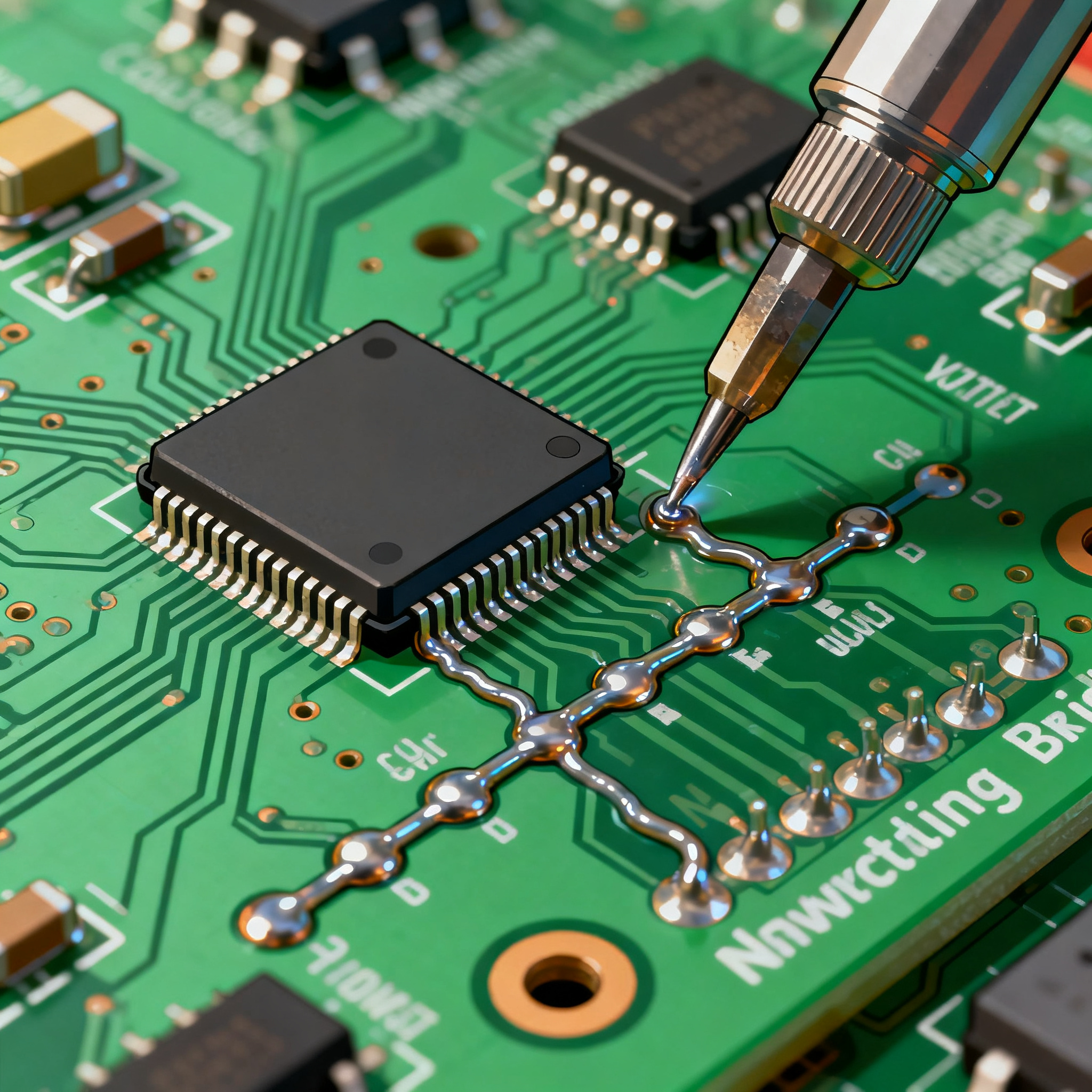
- Solder Bridges: Caused by excess solder creating unintended connections. Solution: Use appropriate soldering techniques and solder mask to prevent bridging.
- Insufficient Solder: Results in weak connections. Solution: Apply the correct amount of solder and use flux to improve solder flow.
- Component Misalignment: Leads to poor electrical contact. Solution: Use precise component placement and automated pick-and-place machines.
- Solder Balling: Occurs when solder balls form on the board surface. Solution: Optimize reflow profiles and ensure proper cleaning of the board.
- Pad Lift: Happens when pads detach from the board. Solution: Use proper pad design and ensure the board is adequately supported during soldering.
Addressing these issues at the design and assembly stages is crucial for minimizing defects and ensuring the reliability of the final product.
Applications & Use Cases
PCBs are integral to a wide range of applications, from consumer electronics to advanced computing systems. In consumer electronics, PCBs enable compact and efficient designs, supporting devices like smartphones and tablets. In industrial applications, PCBs provide robust and reliable connections for automation and control systems. High-performance computing and telecommunications rely on complex multi-layer PCBs to handle high-speed signals and data processing. The versatility of PCBs makes them indispensable across industries, and their design must be tailored to meet the specific demands of each application.
Selection & Sourcing Guide
When selecting and sourcing PCBs, it's essential to consider factors such as material properties, layer count, and manufacturing capabilities. Collaborating with reputable suppliers and manufacturers ensures access to high-quality materials and advanced production techniques. For sourcing components and materials, consider using platforms like IC Online, which offers a wide range of electronic components and materials to meet diverse design requirements.
FAQ
- What is the importance of trace width in PCB design? Trace width is crucial for determining the current-carrying capacity of the PCB. Wider traces can handle more current, reducing resistance and heat generation.
- How does layer stackup affect PCB performance? Layer stackup influences impedance control, signal integrity, and thermal management. Proper stackup design ensures reliable signal transmission and effective heat dissipation.
- What materials are best for high-frequency applications? Materials like Rogers 4350B and Teflon are ideal for high-frequency applications due to their low dielectric constants and loss tangents.
- How can I prevent solder bridges during assembly? Use solder masks to define soldering areas and apply appropriate soldering techniques to prevent excess solder from forming bridges.
- What is the role of a design rule check (DRC)? A DRC ensures that the PCB layout complies with design specifications and manufacturability guidelines, helping to identify potential defects before fabrication.
- How can I ensure effective thermal management in my PCB design? Incorporate thermal vias, heat sinks, and appropriate material selection to effectively manage heat dissipation and prevent overheating.
- What are the common causes of pad lift, and how can it be prevented? Pad lift can be caused by insufficient adhesion or mechanical stress. Ensure proper pad design and support during soldering to prevent this defect.
- Why is signal integrity important in PCB design? Signal integrity ensures that signals are transmitted with minimal distortion and loss, which is crucial for high-speed and high-frequency applications.
- How do I choose the right PCB manufacturer? Consider factors such as manufacturing capabilities, quality standards, and turnaround time. Collaborate with manufacturers who align with your design requirements and production volume.
- What are the benefits of using controlled impedance in PCB design? Controlled impedance is essential for maintaining signal integrity in high-speed applications, reducing reflections and ensuring accurate signal transmission.
Conclusion
Achieving flawless connections in PCBA requires a comprehensive understanding of design principles, material properties, and manufacturing techniques. By adhering to PCB layout rules, selecting appropriate stackup configurations, and considering material properties, engineers can minimize soldering defects and enhance board performance. This guide provides a foundation for designing reliable and high-quality PCBs, ensuring that electronic devices meet the demands of today's technology-driven world.